Advanced Silicon Substrate Fabrication Process
This detailed guide covers the process for patterning silicon substrates through multiple levels and masks using photolithography and deep RIE. It includes steps such as poly-silicon deposition, oxide layer deposition, resist patterning, and metal removal.

Advanced Silicon Substrate Fabrication Process
E N D
Presentation Transcript
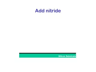
Silicon Substrate Add nitride
Silicon Substrate Add Poly0
Patterned Photoresist Silicon Substrate Patterning through 1st level mask (Poly0)using Photolithography Photoresist
Patterned Photoresist Silicon Substrate Removal of Unwanted Poly0 using Reactive Ion Etching
Silicon Substrate 1st Oxide Deposition using LPCVD
Silicon Substrate Patterning through 2nd level mask (Dimple)using Photolithography... and Deep RIE Photoresist
Silicon Substrate Patterning through 3rd level mask (Anchor)using Photolithography and Deep RIE Photoresist
Silicon Substrate Blanket un-doped polysilicon deposition(Poly1) using LPCVD... followed by PSG deposition and annealing
Silicon Substrate Patterning through 4th level mask (Poly1) using Photolithography... and Deep RIE Photoresist
Silicon Substrate Deposition of 2nd Oxide Layer
Silicon Substrate Patterning through 5th level mask using photolithography and deep RIE
Silicon Substrate Patterning through 6th level mask using photolithography and deep RIE
Silicon Substrate Deposition of undoped polysilicon, followed by PSG hardmask layer, then anneal
Silicon Substrate Patterning through 7th level mask using photolithography and deep RIE
Silicon Substrate Patterning through 8th level mask using photolithography and liftoff, followed by removal of unwanted resist and metal in solvent bath
Release of structures using HF Silicon Substrate