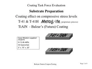
Substrate Preparation Techniques
Substrate Preparation Techniques. Lecture 7 G.J. Mankey gmankey@mint.ua.edu. Types of Substrates. Insulating and Conducting Amorphous and Single Crystal Native Oxide or Passivated Cleaved or Cut Mechanical Polished or Electropolished. Characterization of Substrates. Optical Microscopy

Substrate Preparation Techniques
E N D
Presentation Transcript
Substrate Preparation Techniques Lecture 7 G.J. Mankey gmankey@mint.ua.edu
Types of Substrates • Insulating and Conducting • Amorphous and Single Crystal • Native Oxide or Passivated • Cleaved or Cut • Mechanical Polished or Electropolished
Characterization of Substrates • Optical Microscopy • Atomic Force Microscopy • Spectroscopic Ellipsometry • Electron Diffraction • Auger or X-ray Photoelectron Spectroscopy
Surfaces and Solvents • Never touch the substrate surface without first determining that it must be cleaned or polished before use. • If a solvent wash is necessary verify the purity of the solvent before use. • Do not allow the solvent to form droplets and dry up on the surface--they will redeposit dirt on the surface. • Remember--the best solvents always have dirt dissolved in them, so use them sparingly.
Surface Polishing • For most applications, a surface with a mirror finish is best. • Mechanical polishing should be performed with progressively finer diamond or alumina polishing compound. • The substrate should be thoroughly washed between steps to avoid contamination the polishing compounds. • Leave the polishing area cleaner than when you found it.
Electrochemical Polishing • Refer to Tegart, Electrochemical Polishing Techniques for the proper chemicals and voltages. • Carefully monitor the surface quality with a microscope at small time intervals. • Test the polarities and voltages by polishing a small amount of a test material first. • Always label the electropolishing mixture with the chemical formula and amounts of materials.
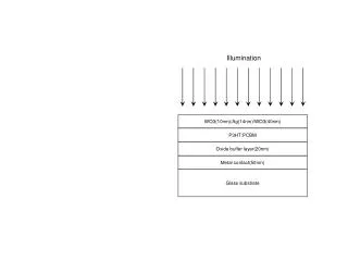
Passivated Surface SiOx • A layer of adsorbate material on the surface that limits further oxidation or corrosion is called the passivation layer. • The layer can be amorphous as in the case of SiOx on Si or crystalline as in the case of H-Si. • If there are defects in the passivation layer, it will be less resistant to corrosion and it will degrade with time. H-Si
Special Techniques • Irradiation with UV light for a day or two to "break up" hydrocarbon contaminants. • CO2 "snow" a jet of frozen particles gently bombard the surface to remove contaminants. • Plasma etching can be used to roughen a surface in a controlled manner.
Single Crystal Surfaces • For thin film deposition only the ordering of the topmost layers matters. • A layer of adsorbed gas or oxide on a single crystal generally prevents epitaxial growth--there are few exceptions to this rule. • Oxide layers on metals usually cannot be removed by annealing alone. • On Si the oxide must be heated to above 800ºC to remove it. • In situ processing, Ar bombardment and/or annealing, is usually required to make a good clean single crystal surface.
Ar Bombardment and Annealing • Bombarding the surface with an energetic beam (500-5000 eV) of Noble gas ions removes contaminated surface layers. • A typical current density of a few microamps per square centimeter will etch a few atomic layers per minute. • Some material is redeposited, so the efficiency of removing contaminant layers is reduced. • Cycles of bombardment and annealing to about 2/3 of the melting point produce a smooth, ordered surface.
Optical Microscopy • Use the optical microscope to check for scratches, spots and dirt. • Use polarized light with the analyzer adjusted to close to extinction to detect small particles and imperfections. • Vary the color of the incident light with the filters to highlight different features.
Atomic Force Microscopy • Characterize the substrate roughness before and after each process step. • Tapping mode is generally the best method for this task. • A good substrate should have a root mean square roughness near the limit of detection (1 nm). • Take scans at different scan sizes to fully characterize roughness scale (0.1, 1, 10, 40 micrometer).
Spectroscopic Ellipsometry • For future determination of film thickness, you must fully characterize the substrate optical properties first. • Take data in the entire wavelength range (240 - 1100nm) to insure future applicability of material optical constants. • Compare a few substrates produced with the same process to identify possible variations.
Electron Diffraction • RHEED and LEED probe only the topmost layers. • An electron diffraction pattern indicates the surface has a periodic atomic arrangement. • The appearance of a diffraction pattern does not guarantee good crystallinity. • Analyze the diffraction pattern according to spot to background intensity ratio, dependence of peak width on energy, and dependence of peak intensity on diffraction conditions.
Auger / XPS • Characterize the chemical composition of surfaces. • Always perform a high statistics scan of the energies for C, N, and O-- these are the main contaminants of most surfaces. • Depth profiling using Ar bombardment can be used to identify the location of contaminants--surface or bulk?