Download
1 / 17
170 likes | 183 Vues
This presentation by Stan Durkin from Ohio State University discusses the Digital Cathode Front End Board (DCFEB) and its optimization for precision position measurement. It covers the design and features of the DCFEB, including its self-triggering capabilities and optimized sampling and digitization processes. The presentation also explores the benefits of using a Digital Cathode Front End Board for the SLHC upgrade.

E N D
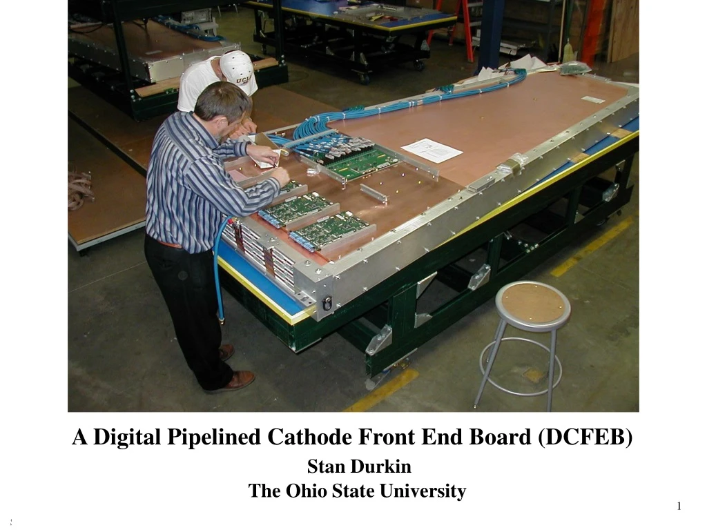
A Digital Pipelined Cathode Front End Board (DCFEB) Stan Durkin The Ohio State University Stan Durkin CMS Upgrade Week
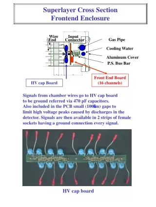
Present Cathode Front End Board (CFEB) Input/Output Optimized for Precision Position Measurement • 5 cfebs/chamber, 96 strips/cfeb • 96 switch capacitors/channel • system is self triggering BUCKEYE (ASIC) - amplifies and shapes input pulse SCA (ASIC) - analog storage for 20 MHz sampled input pulse ADC - events with LVL1ACC digitized and sent to DAQ Motherboard (25 nsec/word) Comparator ASIC - generates trigger hit primitives from shaped pulse Controller FPGA - controls SCA storage and digitization Stan Durkin CMS Upgrade Week
CFEB 50 nsec Sampling and Digitization • 6 Buckeyes serve 6 planes x 16 strips • 6 SCA’s serve 96 strips with 96 caps each • 50 nsec/sampling • no pedestals (< 1%) • 6 ADC’s (150 nsec digitization) • 12-bit + overflow bit • output 1 strip charge/25 nsec • 8 samples digitized for each of 96 strips • 6 SCA’s (96 caps/strip) • LVDS signaling • no cap pedestals • Control FPGA • 12 blocks of 8 caps each • grey-code (1 bit flip) addressing • (see movie for algorithm) Each Strip Amplifier Charge stored every 50 nsec in capacitors Beam Crossing PreLCT L1A·LCT Done 0.8sec 2.2sec 26sec 16 Cap Delay Cap Storage (Poisson) Cap Digization (Queue) For L1ALCT use LCT to choose which 8 capacitors to digitize Caps can be used for storage when all others in use 16 caps set aside for possible use Stan Durkin CMS Upgrade Week
Simulation Single Strip Capacitor Usage A Nontrivial FPGA Algorithm 8 capacitors/block Green – recently used Blue – set aside waiting for L1A Red- digitizing Stan Durkin CMS Upgrade Week
Data Bottlenecks in CSC DAQ at SLHC • CFEB’s 96 Capacitors/channel is main DAQ rate limiter • DCC’s SLINK-64 is second DAQ rate limiter (configurable) Simple Model CFEB Capacitor Storage Transfer to DMB Complete Beam Crossing LCT L1A·LCT 0.8sec 2.2sec 26sec 16 Cap Delay Cap Storage (Poisson) Cap Digization (Queue) Caps can be used for storage when all others in use For SLHC this is the main capacitor usage Stan Durkin CMS Upgrade Week
Time (50ns/bin) Strip Channels Neutron/Gamma Event from X5 Beam test (Aug 99) Random coincidence between L1A and Neutron/Gamma Background Dominates Rate Stan Durkin CMS Upgrade Week
SCA Occupancy: LHC Rate Assumptions L1 Accept: 100 kHz LCT rate: 69 kHz per CFEB (worst case – ME1/1) Estimated LCT rate for 10**34 lumi (D. Acosta et al, 2001) Chamber Type LCT rate per CFEB (kHz) ME1/1 69 ME1/2 4 ME1/3 2 ME2/1 21 ME2/2 3 ME3/1 11 ME3/2 2 ME4/1 8 ME4/2 9 L1-LCT coincidence rate per CFEB: 100 kHz x 70 kHz x 75 ns = 0.5 kH Digitization time (with 6 ADCs on each CFEB) 16 channels x 16 samples/channel x 100 ns = 26 ms Note: This is Monte Carlo, We haven’t measure rates yet! Problem! ‘ME1/1 LCT 96kHz/chamber (20 kHz) CMS Note 2002-007’ Hauser Stan Durkin CMS Upgrade Week
ME1/1 Effective SCA Buffer Occupancy at SLHC • At SLHC: use same L1 accept rate assuming rates go up linearly. Maximum LCT rate is 700 kHz (ME1/1), L1-LCT match rate is 5.25 kHz. • Average number of LCTs during 5.2 ms (=6ms-0.8ms) holding time for 2-blocks: h=5.2x10-6x700x103=3.64 • Average number of L1-LCT matches during 26 ms digitization time: r=26x10-6x5.25x103=0.1365 • Probability of overuse of SCA: 0.09 !!!!!!!!! Stan Durkin CMS Upgrade Week
Digital CFEB – A Nice Idea for the SLHC • Replace Conventional ADC and SCA storage with • Flash ADC and Digital Storage • New System Deadtimeless, Removes rate worries • Similar cost to old system • Fairly Radical Design – Couldn’t build 8 Years Ago Stan Durkin CMS Upgrade Week
Besides Deadtimeless there are other Advantages • Fix ME1/1 Ganged Strips • Removes ganged strips in ME1/1a (aka ME1/4) • Gets rid of ghost tracks trigger and offline • software • Requires 7 DCFEBs per ME1/1 Chamber =1.5 =2.0 =2.4 Improve Cathode Trigger Primitives • presently an ASIC chip • do digitally on new board Cathode charges Stan Durkin CMS Upgrade Week
Overall Scope of Upgrade ME1/1 Electronics Upgrade 504 DCFEBs 72 DMBs 72 TMB (d.c.) 12 MPC 72 LVDB (+more power) 72 LVMB 1008 Cables (default skewclear) LVDB Stan Durkin CMS Upgrade Week
Evaluation of Flash ADCs (B. Bylsma O.S.U) ADC choices:(8 ch, 12 bit, 20-65 MSPS, Serial LVDS output) • MAX1437(Maxim) 1.8V supply, 1.4Vpp range • ADC12EU050(National) 1.2V supply, 2.1Vpp range • AD9222 (Analog Devices) 1.8V supply, 2Vpp range • ADS5281 (Texas Instr.) 3.3V analog, 1.8V digital, 2Vpp range Stan Durkin CMS Upgrade Week
Flash ADC/Amplifier Coupling Issues No Flash ADC is a drop-in replacements for SCA/ADC • ADC’s • All have differential inputs • Limits on common mode • Have internal input bias network • Pre-Amp • Single ended output • Limited range of baseline level • Designed to drive small capacitive load • Pre-Amp/ADC Interface • Mnfr. suggest transformer coupling • (not an option for us) • Amplifier to generate differential signal • (requires 96 amplifiers) • Direct couple single ended signal • (common mode consequences) • (level shifting/scaling) • AC couple single ended signal • (common mode consequences) • (no level shifting, but still have biasing to consider Stan Durkin CMS Upgrade Week
Common Mode Constraints (ADS5281) Direct Coupling Difficult Common Mode • Data Sheet: Vcm = 1.5±0.05V • How far from nominal? • Baseline Level • Range • Digital output range is 2V • But is linear range of common mode 2V • ADC Constraints: • Vcm -600mV < (IN+ + IN-)/2 < Vcm +300mV (1.8Vpp on IN+) • (IN- -1V) < IN+ < (IN-+1V) (ADC output range) • Pre-Amp Constraints: • Baseline Level • Currently 1.8V • Max ~2.0V • Min ~1.2V (maybe 1.0V) • Drive Capability • Small (few mA at best) • Scaling: • Scale down input • Add digital gain on output • Resistor divider Stan Durkin CMS Upgrade Week
DCFEB R&D plans Buckeye Amp -> ADC5281 Evaluation Board • Preliminary Tests are Encouraging • Flash ADC sensitive to common mode gain • Need R&D board to fully test coupling and noise 50 nsec Samples Short Term Goal: Install Prototype System on a ME4/2 Chamber during 2012 Shutdown • DCFEB Critical Item so Divide Labor (Generic R&D) • DCFEB R&D Board, OSU • FPGA Firmware, Florida • Virtex 6 R&D Board, TAMU • Virtex 6 Radiation Testing, NEU • Optical Cable Interface DCFEBDMB/TMB Stan Durkin CMS Upgrade Week
DCFEB R&D Board Designed to study (there will be issues): - Coupling single ended Buckeye Amp to bipolar flash SCAs - Linearity/Shape … Noise on Analog-Digital boards can be problems - use old PC board’s analog isolation Stan Durkin CMS Upgrade Week
Conclusions DCFEB R&D Board Available Late this Summer Then: - noise tests - linearity/pulse shape tests - radiation tests, SEU and lifetime measurements If all goes well layout and schematics of a DCFEB Prototype board will start late Fall Stan Durkin CMS Upgrade Week