Front-end board design
170 likes | 351 Vues
Front-end board design. Cagliari is responsible for front-end board prototyping and production. (we already designed and produced boards for CARIOCA8 and CARIOCA9)

Front-end board design
E N D
Presentation Transcript
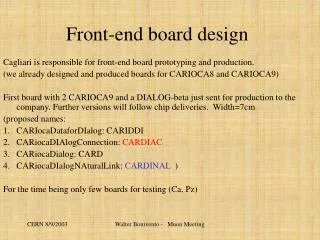
Front-end board design Cagliari is responsible for front-end board prototyping and production. (we already designed and produced boards for CARIOCA8 and CARIOCA9) First board with 2 CARIOCA9 and a DIALOG-beta just sent for production to the company. Further versions will follow chip deliveries. Width=7cm (proposed names: • CARIocaDataforDIalog: CARIDDI • CARiocaDIAlogConnection: CARDIAC • CARiocaDialog: CARD • CARiocaDIalogNAturalLink: CARDINAL ) For the time being only few boards for testing (Ca, Pz) Walter Bonivento - Muon Meeting
Front-end board design • 6 layer PCB: 2 plane layers (power and ground) and 4 connection layers. • The design was made trying to use as much as possible the same layout technics used in the previous carioca boards (grounding, components placing, etc.) • 2 opamps to buffer threshold lines (one per chip) Walter Bonivento - Muon Meeting
Front-end board design Layout of the board: • On the top layer (outer side): • Dialog • Power connector • Output connector • I2C connectors • On the bottom layer (inner side): • Carioca chips. • Input connectors. • LVDS terminations (outputs of the two Carioca). Walter Bonivento - Muon Meeting
Front-end board design D.Marras (Ca) PCB Layout Walter Bonivento - Muon Meeting
Front-end board design • CARIOCA10 board (no DIALOG) designed in Ca and produced at CERN. • CARIOCA10 tests will be done by CERN group • CARIOCA10 +DIALOGbeta board will be done asap in Ca. It might be produced (if working) in larger number for chamber testing (also GEM). Threshold range of DIALOG enough (threshold DAC 10mV resolution; 15mV/fC CARIOCA)? Width=6.5cm • CARIOCA10+final DIALOG will follow just after DIALOG submission A first price estimation for the production will be done in a short time (when mounting components..). Potenza is responsible for spark protection board production. LNF already designed a version which can be also of width=6.5cm. LNF will produce adapter from chamber to SPB Walter Bonivento - Muon Meeting
Front-end board testing We have to test: a) chips one by one b)FEB one by one Strategy depends on CARIOCA chip testing: who does it? Who pays for? What kind of test is done: extensive, coarse? Manpower… In principle CERN (as responsible for chip production) but… THIS WILL INFLUENCE WHAT FOLLOWS VERY MUCH so take what follows as as ideas to be discussed here Walter Bonivento - Muon Meeting
Front-end board testing 2 groups developed so far test working set-ups for FEB testing (only front-end chips) and results were compared on few boards and found to be similar: • Potenza: setup with laboratory equipment a) commercial pulse injector b) varcap (diodes) on input (!) c) VME readout d) labview program They do S-curves on all channels in 1min/board Time measurements can be easily implemented with a VME TDC Checks to be done with some CARIOCA boards tested by Werner to see compatibility. Walter Bonivento - Muon Meeting
Front-end board testing 2 Rio: developed a home-made boards doing all the tests of S-curves + rate method They did not implemented time measurement Schematics on the next page time per measurement ? Walter Bonivento - Muon Meeting
Hardware Schematic of Rio setup INJECTION BOARD • controlled parameters: • injected charge • threshold value • channel to be injected • frequency of injection • time window to count • injection polarity 74F38 channel injection line 16 channels charge value … supply bus CONTROLLING BOARD FPGA front-end board channels 0 to 7 counters mux readout PC interface NI-DAQ enable channels 8 to 15 select reset • NI-DAQ main features: • 2 DACs (12 bits) • 2 Counters (24 bits) • 3 8-bits I/O ports Walter Bonivento - Muon Meeting
Front-end board testing Now we have to include the DIALOG in the tests. Proposal: we combine experience of both groups and produce updated versions of the test bench for FEB with the idea of migrating towards LHCb system components more and more (also to be able to do system tests like in the experiment) Test bench will be in Potenza and they are “responsible” for the series test Version 1 : Potenza now + DIALOG thesholds and masks set by one service board and C program (1 month from now) (Valerio-Rafael-…) IN ONE MONTH A WORKING SYSTEM!!! Version 2: Potenza now+ service board and pulse injection (through NI I/O board) with PVSS/CANBUS and VME output replaced by ODE+TTx (one disadvantage=TDC of SYNC has 1.5ns resolution but it might be enough for series test) (Valerio-Rafael-…) Walter Bonivento - Muon Meeting
Complete test system • Test Dialog and Carioca using I2c_lvds • Test FE input connection and and carioca response depending from input capacitor. • Measure time using ODE boards • (need ttc system) Potenza Inj board with varicap system Analog Signals I2c_lvds FE board LVDS Signals NI I/O Board PVSS With FEET procedure ODE Board (time measurement) Service Board Canbus Walter Bonivento - Muon Meeting Valerio Bocci 2003
Front-end board testing We (Rome I) would also be able to use features which will be used in the experiment: 1) Charge injection in the CARIOCA from the DIALOG 2) Scaler readout from the DIALOG Need improvements in the DIALOG: one counter/channel 32 bit (now 8…) and DACs for charge injection. Walter Bonivento - Muon Meeting
Self Test of the Carioca-Dialog system (Using Dialog & Service Board facility) • Only one conection (i2c_lvds) • The system can test : board connectivity,carioca channel response,dialog and Carioca functionality • The input and spark protection are not tested • The LVDS output are not tested Spark+Input Carioca Carioca Service Board Dialog I2c_lvds+ctrl signals CANbus Output LVDS PC Running PVSS (FEET Procedures) Carioca threshold,pulse,charge dac Signal processed from carioca(Analog) and then from dialog (digital) I2c lvds+pulse signal Walter Bonivento - Muon Meeting Valerio Bocci 2003
Front-end board testing Of course scenario changes if we (Italy) have also to test CARIOCAs. Walter Bonivento - Muon Meeting
ELECTRONICS SCHEDULE AND MILESTONES Walter Bonivento - Muon Meeting
LV distribution GEM-LNF Walter Bonivento - Muon Meeting
LVDS ground cut Scintillator Coincidence trigger HV ground cut One LV line filtered with hf transformer One ground line to HV power supply + DAQ + earth Floating LV Incoming ground from LV Walter Bonivento - Muon Meeting