SPINTRONICS
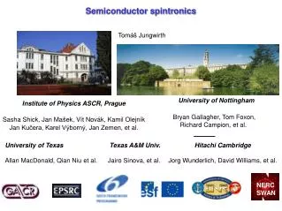
SPINTRONICS. Tom áš Jungwirth. Universit y of Nottingham. Fyzikální ústav AVČR. 1. Current s pi ntronics in HDD read-heads and memory chips 2. Physical principles of operation of current spintronic devices 3. Research at the frontiers of s pintroni cs 4. Summary.

SPINTRONICS
E N D
Presentation Transcript
SPINTRONICS Tomáš Jungwirth University of Nottingham Fyzikální ústav AVČR
1. Current spintronics in HDD read-heads and memory chips 2.Physical principles of operation of current spintronic devices 3. Research at the frontiers of spintronics 4. Summary
Current spintronics applications First hard disc(1956) - classical electronics for read-out 1 bit: 1mm x 1mm MByte From PC hard drives ('90) to micro-discs - spintronic read-heads 1 bit: 10-3mm x 10-3mm GByte
HARD DISK DRIVE READ HEADS spintronic read heads horse-shoe read/write heads
Anisotropic magnetoresistance (AMR) read head 1992 - dawn of spintronics Appreciable sensitivity, simple design, scalable, cheap
Giant magnetoresistance (GMR) read head 1997 High sensitivity
MEMORY CHIPS .DRAM(capacitor) - high density, cheep x slow, high power, volatile .SRAM(transistors) - low power, fast x low density, expensive, volatile .Flash (floating gate) - non-volatilex slow, limited life, expensive Operation through electron chargemanipulation
MRAM – universal memory fast, small, non-volatile First commercial 4Mb MRAM Tunneling magneto-resistance effect (TMR) RAM chip that won't forget ↓ instant on-and-off computers
MRAM – universal memory fast, small, non-volatile First commercial 4Mb MRAM Tunneling magneto-resistance effect (TMR) RAM chip that won't forget ↓ instant on-and-off computers
1. Current spintronics in HDD read-heads and memory chips 2.Physical principles of current spintronic devices operation 3. Research at the frontiers of spintronics 4. Summary
Electron has a charge (electronics) and spin (spintronics) Electrons do not actually “spin”, they produce a magnetic moment that is equivalent to an electron spinning clockwise or anti-clockwise
quantum mechanics & special relativity particles/antiparticles & spin Dirac eq. E=p2/2m E ih d/dt p -ih d/dr . . . E2/c2=p2+m2c2 (E=mc2 for p=0) high-energy physics solid-state physics and microelectronics
e- Resistor classical spintronic external manipulation of charge & spin internal communication between charge & spin
total wf antisymmetric = * spin wf symmetric (aligned) orbital wf antisymmetric e- FERO MAG NET Non-relativistic (except for the spin) many-body Pauli exclusion principle & Coulomb repulsionFerromagnetism • Robust(can be as strong as bonding in solids) • Strong coupling to magnetic field • (weak fields = anisotropy fields needed • only to reorient macroscopic moment)
p s V e- Beff Relativistic "single-particle" Spin-orbit coupling (Dirac eq. in external field V(r) & 2nd-order in v /c around non-relativistic limit) Produces an electric field Ingredients: - potential V(r) - motion of an electron E In the rest frame of an electron the electric field generates and effective magnetic field - gives an effective interaction with the electron’s magnetic moment • Current sensitive to magnetization • direction
ky kx p s V e- Beff Spintronics Ferromagnetism Coulomb repulsion & Pauli exclusion principle Spin-orbit coupling Dirac eq. in external field V(r) & 2nd-order in v /c around non-relativistic limit Fermi surfaces ~(k . s)2 + Mx . sx ~(k . s)2 ~Mx . sx FM without SO-coupling SO-coupling without FM FM & SO-coupling
ky kx Fermi surfaces ~(k . s)2 + Mx . sx ~(k . s)2 ~Mx . sx FM & SO-coupling FM without SO-coupling SO-coupling without FM AMR M Ferromagnetism: sensitivity to magnetic field SO-coupling: anisotropies in Ohmic transport characteristics; ~1-10% MR sensor scattering ky kx M ky kx hot spots for scattering of states moving M R(M I)> R(M || I)
Diode classical spin-valve TMR Based on ferromagnetism only; ~100% MR sensor or memory no (few) spin-up DOS available at EF large spin-up DOS available at EF
1. Current spintronics in HDD read-heads and memory chips 2.Physical principles of current spintronic devices operation 3. Research at the frontiers of spintronics 4. Summary
EXTERNAL MAGNETIC FIELD problems with integration - extra wires, addressing neighboring bits
Current (instead of magnetic field) induced switching Angular momentum conservation spin-torque
magnetic field current Myers et al., Science '99; PRL '02 local, reliable, but fairly large currents needed Likely the future of MRAMs
Spintronics in the footsteps of classical electronics from resistors and diodes to transistors
AMR based diode - TAMR sensor/memory elemets TAMR TMR no need for exchange biasing or spin coherent tunneling Au FM AFM Simpler design without exchange-biasing the fixed magnet contact
Spintronic transistor based on AMR type of effect Huge, gatable, and hysteretic MR Single-electron transistor Two "gates": electric and magnetic
M [010] [110] F Q VD [100] Source Drain [110] [010] Gate VG Q0 Q0 e2/2C Spintronic transistor based on CBAMR magnetic electric & SO-coupling (M) control of Coulomb blockade oscillations
CBAMR SET • Generic effect in FMs with SO-coupling • Combines electrical transistor action • with magnetic storage • Switching between p-type and n-type transistor • by M programmable logic In principle feasible but difficult to realize at room temperature
Spintronics in the footsteps of classical electronics from metals to semiconductors
p s V Beff Spin FET – spin injection from ferromagnet & SO coupling in semiconductor Difficulties with injecting spin polarized currents from metal ferromagnets to semiconductors, with spin-coherence, etc. not yet realized
Ga Mn As Mn Ferromagnetic semiconductors – all semiconductor spintronics More tricky than just hammering an iron nail in a silicon wafer GaAs - standard semiconductor Mn - dilute magnetic element (Ga,Mn)As - ferromagnetic semiconductor
Ga Mn As Mn (Ga,Mn)As (and other III-Mn-V) ferromagnetic semiconductor • compatible with conventional III-V semiconductors (GaAs) • dilute moment system e.g., low currents needed for writing • Mn-Mn coupling mediated by spin-polarized delocalized holes spintronics • tunability of magnetic properties as in the more conventional semiconductor electronic properties. • strong spin-orbit coupling magnetic and magnetotransport anisotropies • Mn-doping (group II for III substitution) limited to ~10% • p-type doping only • maximum Curie temperature below 200 K
Ga Mn As Mn (Ga,Mn)As material 5 d-electrons with L=0 S=5/2 local moment moderately shallow acceptor (110 meV) hole -Mn local moments too dilute (near-neghbors cople AF) - Holes do not polarize in pure GaAs - Hole mediated Mn-Mn FM coupling
Ga Mn As Mn Mn–hole spin-spin interaction As-p Mn-d hybridization Hybridization like-spin level repulsion Jpd SMn shole interaction
Mn As Ga Ferromagnetic Mn-Mn coupling mediated by holes heff = Jpd <SMn> || x Hole Fermi surfaces Heff = Jpd <shole> || -x
No apparent physical barriers for achieving room Tc in III-Mn-V or related functional dilute moment ferromagnetic semiconductors Need to combine detailed understanding of physics and technology Impurity-band holes short-range coupl. Delocalized holes long-range coupl. Weak hybrid. Strong hybrid. InSb, InAs, GaAs d5 GaP
And look into related semiconductor host families like e.g. I-II-V’s III = I + II Ga = Li + Zn • GaAs and LiZnAs are twin SC • (Ga,Mn)As and Li(Zn,Mn)As • should be twin ferromagnetic SC • But Mn isovalent in Li(Zn,Mn)As • no Mn concentration limit • possibly both p-type and n-type ferromagnetic SC
Spintronics in non-magnetic semiconductors way around the problem of Tc in ferromagnetic semiconductors & back to exploring spintronics fundamentals
V Spintronics relies on extraordinary magnetoresistance Ordinary magnetoresistance: response in normal metals to external magnetic field via classical Lorentz force Extraordinary magnetoresistance: response to internal spin polarization in ferromagnets often via quantum-relativistic spin-orbit coupling B anisotropic magnetoresistance _ _ _ _ _ _ _ _ _ _ _ FL + + + + + + + + + + + + + I V _ _ FSO M _ I e.g. ordinary (quantum) Hall effect and anomalous Hall effect Known for more than 100 years but still controversial
_ _ _ FSO _ non-magnetic FSO I majority _ _ _ FSO _ FSO I minority V V=0 Anomalous Hall effect in ferromagnetic conductors: spin-dependent deflection & more spin-ups transverse voltage skew scattering side jump intrinsic Spin Hall effect in non-magnetic conductors: spin-dependent deflection transverse edge spin polarization
n p n Cu Spin Hall effect detected optically in GaAs-based structures Same magnetization achieved by external field generated by a superconducting magnet with 106 x larger dimensions & 106 x larger currents SHE mikročip, 100A supravodivý magnet, 100 A SHE edge spin accumulation can be extracted and moved further into the circuit SHE detected elecrically in metals
1. Current spintronics in HDD read-heads and memory chips 2.Physical principles of current spintronic devices operation 3. Research at the frontiers of spintronics 4. Summary
Downscaling approach about to expire currently ~ 30 nm feature size interatomic distance in ~20 years • Spintronics: from straighforward downscaling to • more "intelligent" device concepts: • simpler more efficient realization for a given functionality (AMR sensor) • multifunctional (integrated reading, writing, and processing) • new materials (ferromagnetic semiconductors) • fundamental understanding of quantum-relativistic electron transport (extraordinary MR)
Ferro Magnetization Current Anisotropic magneto-resistance sensor Electromagnet • Information reading • Information reading & storage Tunneling magneto-resistance sensor and memory bit • Information reading & storage & writing Current induced magnetization rotation
Ga Mn As Mn • Information reading & storage & writing & processing Spintronic single-electron transistor: magnetoresistance controlled by gate voltage • New materials Dilute moment ferromagnetic semiconductors • Spintronics fundamentals AMR, anomalous and spin Hall effects