Tunneling Devices
Tunneling Devices. Motivation. Scaling : some proposed tunneling field effect transistor (TFET) designs do not suffer from short channel effects Power Dissipation: TFETs can beat the 60 mV/decade sub-threshold swing of MOSFETs Design Flexibility: Circuits can be made with fewer devices.

Tunneling Devices
E N D
Presentation Transcript
Motivation • Scaling: some proposed tunneling field effect transistor (TFET) designs do not suffer from short channel effects • Power Dissipation: TFETs can beat the 60 mV/decade sub-threshold swing of MOSFETs • Design Flexibility: Circuits can be made with fewer devices
human brain in 2012? Obligatory Moore’s Law Reference http://www.intel.com/research/silicon/mooreslaw.htm
What’s so great about a tunneling device? • Lower sub-threshold swing can allow for lower operating voltages to be used • Negative differential resistance (NDR) properties can be exploited to create simpler designs for bi-stable circuits, differential comparators, oscillators, etc. • Leads to chips that consume less power
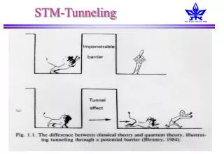
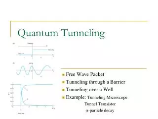
Tunneling • Tunneling is a quantum mechanical phenomenon with no analog in classical physics • Occurs when an electron passes through a potential barrier without having enough energy to do so
(Esaki) Tunnel Diode (TD) EC EV EF • Simplest tunneling device • Heavily-doped pn junction • Leads to overlap of conduction and valence bands • Carriers are able to tunnel inter-band • Tunneling goes exponentially with tunneling distance • Requires junction to be abrupt
Band-to-Band Tunneling in a Tunnel Diode (c) (e) I (b) (d) V EC (a) EV EF (a) (b) (c) (d) (e)
I V Figures of Merit Peak current 100 kA/cm2 Peak-to-Valley Ratio (PVR)
Bi-stable Configuration V I D1 X D2 X1 X2 V
TD Differential Comparator VCC D3 D4 CK X M3 M4 D1 D2 VOUT VOUT VIN VIN RL RL M1 M2 I1 I2 ITAIL -VEE
Direct vs. Indirect Tunneling Indirect Direct Indirect materials require phonons to tunnel, thus reducing the probability of a tunneling event


