Download
1 / 23
230 likes | 509 Vues
Discover the fundamentals of light emitting diodes (LEDs) and their semiconductor technology, including band gaps, energy transitions, and injection electroluminescence mechanics. Learn how LEDs emit light based on band gap energy, electron-hole recombinations, and the structure of pn junction diodes. Explore the principles behind LED operation, including heavily doped n-type semiconductors, energy band diagrams, and device structures. Dive into the mechanisms of photon emission, electron diffusion barriers, and photon reabsorption prevention. Unravel the intricate design and functionality of LEDs for efficient light emission.

E N D
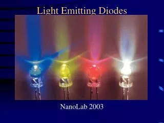
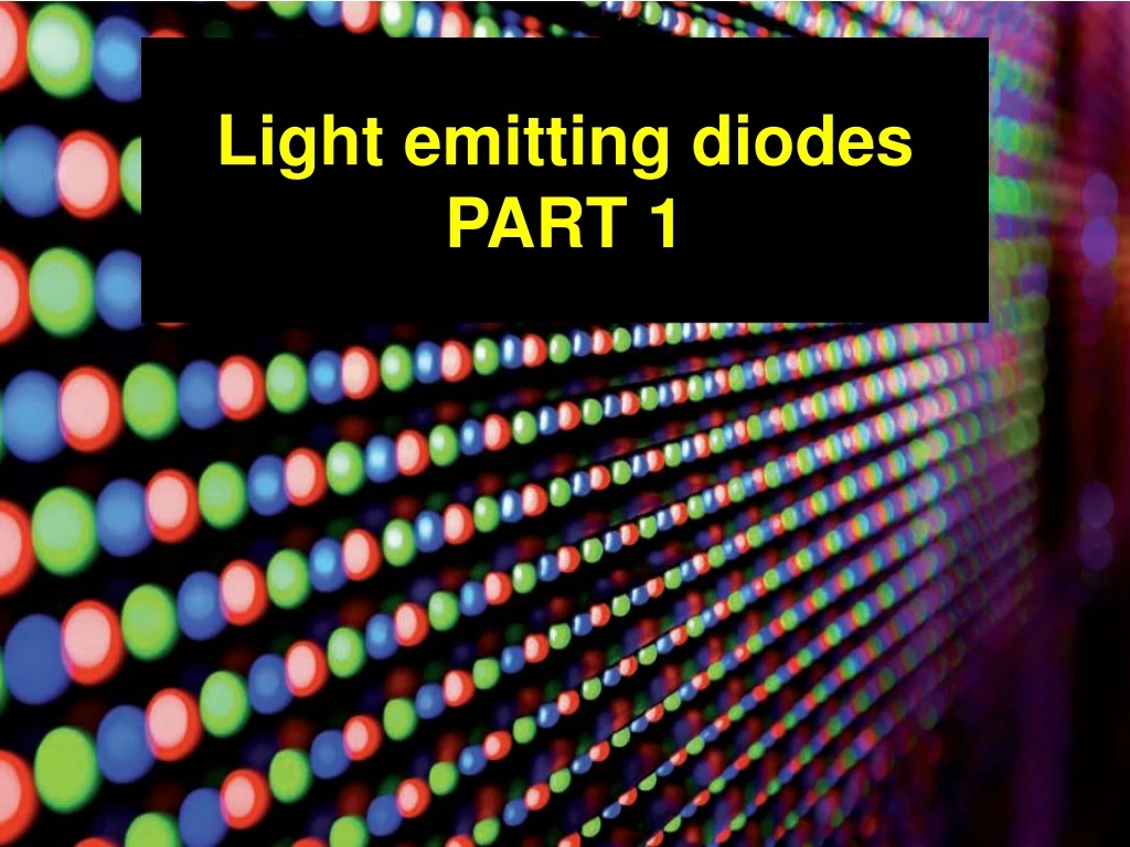
Light emitting diodes PART 1 Light emitting diodes Part 1
What is LED? Semiconductors bring quality to light! LED are semiconductor p-n junctions that under forward bias conditions can emit radiation by electroluminescence in the UV, visible or infrared regions of the electromagnetic spectrum. The qaunta of light energy released is approximately proportional to the band gap of the semiconductor.
When the electron falls down from conduction band and fills in a hole in valence band, there is an obvious loss of energy. CB VB The question is; where does that energy go?
Thus, for a direct band gap material, the excess energy of the electron-hole recombination can either be taken away as heat, or more likely, as a photon of light. • This radiative transition then conserves energy and momentum by giving off light whenever an electron and hole recombine. CB This gives rise to (for us) a new type of device; the light emitting diode (LED). VB
e- e- Mechanism behind photon emission in LEDs? Mechanism is “injection Electroluminescence”. Luminescence part tells us that we are producing photons. Electro part tells us that the photons are being produced by an electric current. Injection tells us that photon production is by the injection of current carriers.
Producing photon Electrons recombine with holes. e- h CB Energy of photon is the energy of band gap. VB
Principles heavily n-type dopes potential energy barrier • Essentially a pn junction diode typically made from a direct bandgap semiconductor e.g. GaAs • Electron-hole pair (EHP) recombination results in the emission of a photon – energy equal to the bandgap energy, hv≈Eg • Figure shows energy band diagram on an unbiased pn+ junction device in which the n-side is more heavily doped than the p-side The energy band diagram for p-n+ (heavily n-type dopes) junction without any bias. Built in potential Vo prevents electron From diffusing from n to p side.
Principles • Depletion region extends mainly into the p-side • There is a potential energy barriereV0 from Ec on the n-side to Ec on the p-side, Ec=eV0, V0 is the built-in voltage • Higher concentration of electron in n-side compared to p-side encourages the diffusion of electrons from the n- to the p-side • However the net electron diffusion is prevented by the barrier
As soon as a forward biasV is applied, this voltage drops across the depletion region since this is the most resistive part of the device • Consequently, the built-in potential is reduced to V0-V, which then allows the electron from n-side to diffuse into the p-side • The hole injection component from p to n-side is much smaller than the electron injection component The applied bias reduces V0 and thereby allows electron to diffuse, be injected into p side. Recombination around the junction and within the diffusion length of the electron in the p-side leads to phonon emission
spontaneous emission • Recombination of electrons in the depletion region and the p-side results in spontaneous emission of photons • Recombination primarily in depletion region and volume extending over the diffusion length (Le) of the electrons on the p-side – this recombination zone is called the active region • Phenomenon of light emission from EHP (electron hole pair) recombination as a result of minority carrier injection as in this case is called injection electroluminescence • Statistical nature of recombination leads to emission of photons in random directions – results from spontaneous emission
LED structure has to be such that the emitted photons can escape the device without being reabsorbed by the semiconductor material • This means the p-side has to be sufficiently narrow or we have to use heterostructure devices as will be discussed later
Device structures • The LED structure plays a crucial role in emitting light from the LED surface. The LEDs are structured to ensure most of the recombination's takes place on the surface by the following two ways. 1. By increasing the doping concentration of the substrate, so that additional free minority charge carriers electrons move to the top, recombine and emit light at the surface. 2. By increasing the diffusion length L = √ Dτ, where D is the diffusion coefficient and τ is the carrier life time. But when increased beyond a critical length there is a chance of re-absorption of the photons into the device
Device structures The LED has to be structured so that the photons generated from the device are emitted without being reabsorbed. One solution is to make the p layer on the top thin, enough to create a depletion layer GaAs or GaP
Device structures • LED are typically fabricated by epitaxially growing doped semiconductor layers on a suitable substrate (e.g. GaAs or GaP) as depicted in the next figure • This type of planar pn junction is formed by the epitaxial growth of first the n-layer then the p-layer • Substrate is essentially a mechanical support for the pn junction and can be of different material • The p-side is on the surface from which light is emitted and is therefore made narrow (a few microns) to allow the photons to escape without being reabsorbed • To ensure that most of the recombination is in the p-side , the n-side is heavily doped (n+) • Those photons that are emitted towards the n-side become either absorbed or reflected back at the substrate interface • It is also possible to form p-side by using dopant diffusion
Device structures • Not all light rays reaching the semiconductor-air interface can escape because of total internal reflection (TIR) • Those with angle of incidence greater than the critical anglec become reflected as shown in the next figure • GaAs-air interface, the C = 16o which means that much of the light suffers TIR. • To solve the problem we could: Need to shape the surface of the semiconductor into a dome or hemisphere so that light rays strike the surface at angles less than
C = 16o which means that much of the light suffers TIR reduce TIR
Drawback – difficult to fabricate the dome and associated increase in expense • Inexpensive and common procedure to reduce TIR is encapsulation with a transparent plastic medium that has higher refractive index than air and also has a domed surface on one side of the pn junction
http://www.youtube.com/watch?v=Yd3hzYAJzOo&feature=related • http://www.youtube.com/watch?v=zC9IEX-DzXM&feature=related • http://www.youtube.com/watch?v=D0fBrlj37JU&feature=related • http://www.youtube.com/watch?v=bVBDxjk8T60&feature=related