TDR Technology Overview: Cable Characterization & Testing at Swarthmore College
Learn about Time Domain Reflectometer technology for cable characterization and testing, project goals, equipment architecture, and timing requirements at Swarthmore College's Engineering department. The TDR instrument overview includes methods of characterizing conductors, energy propagation measurement, and more.

TDR Technology Overview: Cable Characterization & Testing at Swarthmore College
E N D
Presentation Transcript
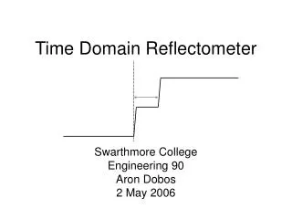
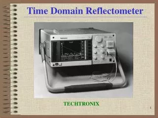
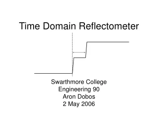
Time Domain Reflectometer Swarthmore College Engineering 90 Aron Dobos 2 May 2006
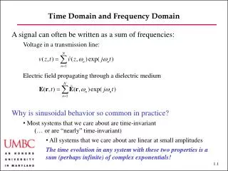
TDR Technology Overview • Method of characterizing conductors and other test mediums by measuring energy propagation through the device under test • Cable characterization, geological survey, groundwater monitoring, oil field localization, structural integrity monitoring • Project goal: TDR instrument for SMA cable characterization
Z0 ZL z = -l z = 0 Transmission Lines • Assume ideal voltage step injected at one end of transmission line with characteristic impedance Z0 • Reflection coefficient at load:
Energy Reflections • Short Circuit: Z0=0, ΓL= -1 : Pulse is reflected with unchanged magnitude but opposite polarity • Open Circuit: Z0=∞, ΓL= 1 : Pulse is reflected with same magnitude and polarity • Matched impedance ZL=Z0, ΓL= 0: No reflection
Equivalent Time Sampling • Stimulus is generated for each data point • Controlled variable time delay between stimulus to the moment the cable voltage is sampled • Energy reflections assumed to reach steady state with zero initial conditions between data points
XFRAME PRETRIGGER SPI{ PC Host Control Interface SCLK SDATA Timebase D/A 40 MHz Osc. PARALLEL INTERFACE CONV_START ADuC7026 SH_DRV A/D Sampler 62k FLASH D/A SMA0 STEP_DRV 8k SRAM POL0 POL1 Step Generator SMA1 EN0 EN1 TDR Instrument Architecture • PC-based host control software • ADuC7026 microcontroller • 2 channel step generator (EN,POL indep.) • Sampler circuit only channel 0 only
Timebase Circuit Overview • Responsible for controlling the precise synchronization between the step generator and sampling circuit • Resolution on order of 10 ps with very low jitter (< 1ps) desired • Implemented as hybrid digital/analog • Digital timer/counters in Xilinx FPGA • Analog DAC-based ramp/comparator
Timing Requirements • Purely digital method is not feasible • for 12 ps resolution, 83 GHz clock required • Purely analog solution is not feasible • Very slow ramp required giving poor jitter performance due to time-uncertainty at the comparison point • 20 MHz clock, 12-bit D/A converter, 50 ns linear ramp 12.2 ps resolution
Sampler Overview • Two stage circuit that very quickly samples the test connector voltage • Provides a proportional voltage to the microcontroller’s A/D converter • Open-loop single-ended topology
Sampler Circuit Charge injected onto C3 provides stimulus for resonant opamp circuit Monostable multivibrator opens SW1 to capture response on C4 Reset by shorting C3 via SW2 2 3 5 4 1 Amplification and offset applied to utilize A/D converter input range Differential strobe pulse opens diode bridge sampling gate briefly at time determined by timebase circuit
Stability and Linearity • Unconditionally stable due to open-loop topology • Linearity not optimal • Sampling gate reverse bias symmetry: DC midpoint value does not track input signal • Differential strobe pulse amplitude and symmetry
Testing • No test cable attached, open circuit • Z0=∞, ΓL= 1 • 3.27 ns RT • ~ 8 in / ns • ~ 13 in cable • ~ correct.
Clock Feedthrough and SNR • Significant 50 ns periodic noise
Acknowledgments • Professor Lynne Molter • Professor Erik Cheever • Ed Jaoudi • Mr. Agoston and Hyperlabs Inc. • Laszlo Dobos