Download
1 / 46
480 likes | 659 Vues
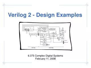
Verilog 2 - Design Examples. 6.375 Complex Digital Systems February 12, 2007. Course administrative notes. If you did not receive an email over the weekend concerning the course then you are not on the student mailing list - please email 6.375-staff Lab 1 is due Friday, February 16

E N D
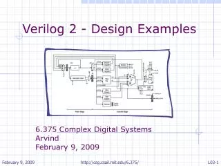
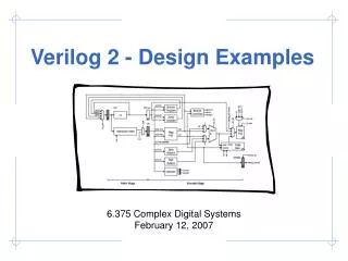
Verilog 2 - Design Examples 6.375 Complex Digital Systems February 12, 2007
Course administrative notes • If you did not receive an email over the weekend concerning the course then you are not on the student mailing list - please email 6.375-staff • Lab 1 is due Friday, February 16 • 2-stage SMIPSv2 processor RTL checked into CVS • Critical thinking questions; hardcopy due in class
Verilog Design Examples • Building blocks • Greatest Common Divisor • Unpipelined SMIPSv1 processor
A module can be described in many different ways but it should not matter from outside Example: mux4
mux4: Gate-level structural Verilog module mux4( input a, b, c, d, input [1:0] sel, output out ); wire [1:0] sel_b; not not0( sel_b[0], sel[0] ); not not1( sel_b[1], sel[1] ); wire n0, n1, n2, n3; and and0( n0, c, sel[1] ); and and1( n1, a, sel_b[1] ); and and2( n2, d, sel[1] ); and and3( n3, b, sel_b[1] ); wire x0, x1; nor nor0( x0, n0, n1 ); nor nor1( x1, n2, n3 ); wire y0, y1; or or0( y0, x0, sel[0] ); or or1( y1, x1, sel_b[0] ); nand nand0( out, y0, y1 ); endmodule sel[0] b d a c sel[1] out
mux4: Using continuous assignments Language defined operators module mux4( input a, b, c, d input [1:0] sel, output out ); wire out, t0, t1; assign out = ~( (t0 | sel[0]) & (t1 | ~sel[0]) ); assign t1 = ~( (sel[1] & d) | (~sel[1] & b) ); assign t0 = ~( (sel[1] & c) | (~sel[1] & a) ); endmodule module mux4( input a, b, c, d input [1:0] sel, output out ); wire out, t0, t1; assign t0 = ~( (sel[1] & c) | (~sel[1] & a) ); assign t1 = ~( (sel[1] & d) | (~sel[1] & b) ); assign out = ~( (t0 | sel[0]) & (t1 | ~sel[0]) ); endmodule The order of these continuous assignment statements does not matter. They essentially happen in parallel!
If input is undefined we want to propagate that information. mux4: Behavioral style // Four input multiplexer module mux4( input a, b, c, d input [1:0] sel, output out ); assign out = ( sel == 0 ) ? a : ( sel == 1 ) ? b : ( sel == 2 ) ? c : ( sel == 3 ) ? d : 1’bx; endmodule
mux4: Using always block module mux4( input a, b, c, d input [1:0] sel, output out ); reg out, t0, t1; always@( a or b or c or d or sel ) begin t0 = ~( (sel[1] & c) | (~sel[1] & a) ); t1 = ~( (sel[1] & d) | (~sel[1] & b) ); out = ~( (t0 | sel[0]) & (t1 | ~sel[0]) ); end endmodule The order of these procedural assignment statements does matter. They essentially happen sequentially!
mux4: Always block permit more advanced sequential idioms module mux4( input a, b, c, d input [1:0] sel, output out ); reg out; always@( * ) begin case ( sel ) 2’d0 : out = a; 2’d1 : out = b; 2’d2 : out = c; 2’d3 : out = d; default : out = 1’bx; endcase end endmodule module mux4( input a, b, c, d input [1:0] sel, output out ); reg out; always@( * ) begin if ( sel == 2’d0 ) out = a; elseif ( sel == 2’d1 ) out = b elseif ( sel == 2’d2 ) out = c elseif ( sel == 2’d3 ) out = d else out = 1’bx; end endmodule Typically we will use always blocks only to describe sequential circuits
default value Parameterized mux4 module mux4#( parameterWIDTH = 1 ) ( input[WIDTH-1:0] a, b, c, d input [1:0] sel, output[WIDTH-1:0] out ); wire [WIDTH-1:0] out, t0, t1; assign t0 = (sel[1]? c : a); assign t1 = (sel[1]? d : b); assign out = (sel[0]? t0: t1); endmodule module mux4( input a, b, c, d input [1:0] sel, output out ); wire out, t0, t1; assign out = ~( (t0 | sel[0]) & (t1 | ~sel[0]) ); assign t1 = ~( (sel[1] & d) | (~sel[1] & b) ); assign t0 = ~( (sel[1] & c) | (~sel[1] & a) ); endmodule Instantiation Syntax mux4#(32) alu_mux ( .a (op1), .b (op2), .c (op3), .d (op4), .sel (alu_mux_sel), .out (alu_mux_out) ); Parameterization is a good practice for reusable modules
next_X X Q D clk next_X X Q D clk enable flip-flops module FF0 (input clk, input d, output q); always @( posedge clk ) begin q <= d; end endmodule module FF (input clk, input d, input en, output q); always @( posedge clk ) begin if ( en ) q <= d; end endmodule
resetN next_X X Q D clk enable flip-flops with reset always @( posedge clk ) begin if (~resetN) Q <= 0; else if ( enable ) Q <= D; end synchronous reset always @( posedge clk or negedge resetN) begin if (~resetN) Q <= 0; else if ( enable ) Q <= D; end What is the difference? asynchronous reset
Register module register#(parameterWIDTH = 1) ( input clk, input [WIDTH-1:0] d, input en, output [WIDTH-1:0] q ); always @( posedge clk ) begin if (en) q <= d; end endmodule
Register in terms of Flipflops module register2 ( input clk, input [1:0] d, input en, output [1:0] q ); always @( posedge clk ) begin if (en) q <= d; end endmodule module register2 ( input clk, input [1:0] d, input en, output [1:0] q ); FF ff0 (.clk(clk), .d(d[0]), .en(en), .q(q[0])); FF ff1 (.clk(clk), .d(d[1]), .en(en), .q(q[1])); endmodule Do they behave the same? yes
genvars disappear after static elaboration Generated names will have regE[i]. prefix Static Elaboration: Generate module register#(parameterWIDTH = 1) ( input clk, input [WIDTH-1:0] d, input en, output [WIDTH-1:0] q ); genvar i; generate for (i =0; i < WIDTH; i = i + 1) begin: regE FF ff(.clk(clk), .d(d[i]), .en(en), .q(q[i])); end endgenerate endmodule
Verilog Design Examples • Building blocks • Greatest Common Divisor • Unpipelined SMIPSv1 processor
GCD in C int GCD( int inA, int inB) { int done = 0; int A = inA; int B = inB; while ( !done ) { if ( A < B ) { swap = A; A = B; B = swap; } elseif ( B != 0 ) A = A - B; else done = 1; } return A; } Such a GCD description can be easily written in Behavioral Verilog It can be simulated but it will have nothing to do with hardware, i.e. it won’t synthesize.
Behavioral GCD in Verilog module gcdGCDUnit_behav#( parameter W = 16 ) ( input[W-1:0] inA, inB, output[W-1:0] out ); reg [W-1:0] A, B, out, swap; integer done; always@(*) begin done = 0; A = inA; B = inB; while ( !done ) begin if ( A < B ) swap = A; A = B; B = swap; elseif ( B != 0 ) A = A - B; else done = 1; end out = A; end endmodule User simply sets the input operands and checks the output; the answer will appear immediately, like a combinational circuit
without some delay out is bogus You have to be careful in using such behavioral models module exGCDTestHarness_behav; reg [15:0] inA, inB; wire [15:0] out; exGCD_behav#(16) gcd_unit( .inA(inA), .inB(inB), .out(out) ); initial begin // 3 = GCD( 27, 15 ) inA = 27; inB = 15; #10; if ( out == 3 ) $display( "Test ( gcd(27,15) ) succeeded, [ %x == %x ]", out, 3 ); else $display( "Test ( gcd(27,15) ) failed, [ %x != %x ]", out, 3 ); $finish; end endmodule
State Less-Than Comparator Equal Comparator Subtractor Deriving an RTL model for GCD module gcdGCDUnit_behav#( parameter W = 16 ) ( input[W-1:0] inA, inB, output[W-1:0] Y ); reg [W-1:0] A, B, Y, swap; integer done; always@(*) begin done = 0; A = inA; B = inB; while ( !done ) begin if ( A < B ) swap = A; A = B; B = swap; elseif ( B != 0 ) A = A - B; else done = 1; end Y = A; end endmodule What does the RTL implementation need?
input_available result_rdy idle result_taken operands_bits_A result_bits_data operands_bits_B clk reset The first step is to carefully design an appropriate port interface
zero? lt A Next develop a datapath which has the proper functional units A = inA; B = inB; while ( !done ) begin if ( A < B ) swap = A; A = B; B = swap; elseif ( B != 0 ) A = A - B; else done = 1; end Y = A; B
zero? lt A Next develop a datapath which has the proper functional units A = inA; B = inB; while ( !done ) begin if ( A < B ) swap = A; A = B; B = swap; elseif ( B != 0 ) A = A - B; else done = 1; end Y = A; B
zero? lt A sub Next develop a datapath which has the proper functional units A = inA; B = inB; while ( !done ) begin if ( A < B ) swap = A; A = B; B = swap; elseif ( B != 0 ) A = A - B; else done = 1; end Y = A; B
A mux sel A reg en B mux sel B reg en B = 0 A < B zero? lt A sub Finally add the control unit to sequence the datapath Control unit is either busy or waiting for input or waitng for out to be picked up A = inA; B = inB; while ( !done ) begin if ( A < B ) swap = A; A = B; B = swap; elseif ( B != 0 ) A = A - B; else done = 1; end Y = A; B
A sel A en B sel B en B = 0 A < B zero? lt A sub B Datapath module interface module gcdGCDUnitDpath_sstr#( parameter W = 16 ) ( input clk, // Data signals input [W-1:0] operands_bits_A, input [W-1:0] operands_bits_B, output [W-1:0] result_bits_data, // Control signals (ctrl->dpath) input A_en, input B_en, input [1:0] A_mux_sel, input B_mux_sel, // Control signals (dpath->ctrl) output B_zero, output A_lt_B );
A sel A en B sel B en B = 0 A < B zero? lt A sub B Connect the modules wire [W-1:0] B; wire [W-1:0] sub_out; wire [W-1:0] A_mux_out; vcMux3#(W) A_mux ( .in0 (operands_bits_A), .in1 (B), .in2 (sub_out), .sel (A_mux_sel), .out (A_mux_out) ); wire [W-1:0] A; vcEDFF_pf#(W) A_pf ( .clk (clk), .en_p (A_en), .d_p (A_mux_out), .q_np (A) );
Using explicit state helps eliminate issues with non-blocking assignments Continuous assignment combinational logic is fine Connect the modules ... wire [W-1:0] B_mux_out; vcMux2#(W) B_mux ( .in0 (operands_bits_B), .in1 (A), .sel (B_mux_sel), .out (B_mux_out) ); vcEDFF_pf#(W) B_pf ( .clk (clk), .en_p (B_en), .d_p (B_mux_out), .q_np (B) ); assign B_zero = ( B == 0 ); assign A_lt_B = ( A < B ); assign sub_out = A - B; assign result_bits_data = A; wire [W-1:0] B; wire [W-1:0] sub_out; wire [W-1:0] A_mux_out; vcMux3#(W) A_mux ( .in0 (operands_bits_A), .in1 (B), .in2 (sub_out), .sel (A_mux_sel), .out (A_mux_out) ); wire [W-1:0] A; vcEDFF_pf#(W) A_pf ( .clk (clk), .en_p (A_en), .d_p (A_mux_out), .q_np (A) );
Control unit requires a simple state machine for valid/ready signals reset WAIT Waiting for new input operands input_availble CALC Swapping and subtracting ( B = 0 ) DONE Waiting for consumer to take the result result_taken
Implementing the control logic finite state machine in Verilog localparam WAIT = 2'd0; localparam CALC = 2'd1; localparam DONE = 2'd2; reg [1:0] state_next; wire [1:0] state; vcRDFF_pf#(2,WAIT) state_pf ( .clk (clk), .reset_p (reset), .d_p (state_next), .q_np (state) ); Localparams are not really parameters at all. They are scoped constants. Explicit state in the control logic is also a good idea!
WAIT : begin A_mux_sel = A_MUX_SEL_IN; A_en = 1'b1; B_mux_sel = B_MUX_SEL_IN; B_en = 1'b1; input_available = 1'b1; end CALC : if ( A_lt_B ) A_mux_sel = A_MUX_SEL_B; A_en = 1'b1; B_mux_sel = B_MUX_SEL_A; B_en = 1'b1; elseif ( !B_zero ) A_mux_sel = A_MUX_SEL_SUB; A_en = 1'b1; end DONE : result_rdy = 1'b1; Implementing the control signal outputs for the finite state machine reg [6:0] cs; always@(*) begin // Default control signals A_mux_sel = A_MUX_SEL_X; A_en = 1'b0; B_mux_sel = B_MUX_SEL_X; B_en = 1'b0; input_available = 1'b0; result_rdy = 1'b0; case ( state ) WAIT : ... CALC : ... DONE : ... endcase end
reset WAIT input_availble CALC ( B = 0 ) DONE result_taken Implementing the state transitionsfor the finite state machine always @(*) begin // Default is to stay in the same state state_next = state; case ( state ) WAIT : if ( input_available ) state_next = CALC; CALC : if ( B_zero ) state_next = DONE; DONE : if ( result_taken ) state_next = WAIT; endcase end
RTL test harness requires proper handling of the ready/valid signals Generic Test Source Generic Test Sink A sel A en B sel B en B = 0 A < B zero? lt A sub B
We can compare the behavioral and RTL implementations to verify correctness Test Inputs Behavioral Model RTL Model Test Outputs Test Outputs Identical?
Verilog Design Examples • Building blocks • Greatest Common Divisor • Unpipelined SMIPSv1 processor
SMIPS is a simple MIPS ISA which includes three variants • SMIPSv1 • 5 instructions • No exceptions/interrupts • Lecture examples • SMIPSv2 • 35 instructions • No exceptions/interrupts • ISA for lab assignments • SMIPSv3 • 58 instructions • Full system coproc with exceptions/Interrupts • Optional ISA for projects
The first step is to carefully design an appropriate port interface
SMIPSv1 Block DiagramHow do we start implementing? Divide and Conquer! Step 1: Identify the memories Step 2: Identify the datapaths Step 3: Everything else is random logic
Let’s identify the memories, datapaths, and random logic in our SMIPSv1 design Divide and Conquer! Step 1: Identify the memories Step 2: Identify the datapaths Step 3: Everything else is random logic
Let’s identify the memories, datapaths, and random logic in our SMIPSv1 design Now identify the signals which will make up the interface between the datapath, memories, and random logic
SMIPSv1 datapath interface contains controls signals and memory data buses module smipsProcDpath_pstr ( input clk, reset, // Memory ports output [31:0] imemreq_bits_addr, output [31:0] dmemreq_bits_addr, output [31:0] dmemreq_bits_data, input [31:0] dmemresp_bits_data, // Controls signals (ctrl->dpath) input pc_mux_sel, input [ 4:0] rf_raddr0, input [ 4:0] rf_raddr1, input rf_wen, input [ 4:0] rf_waddr, input op0_mux_sel, input op1_mux_sel, input [15:0] inst_imm, input wb_mux_sel, // Control signals (dpath->ctrl) output branch_cond_eq, output[7:0] tohost_next ); wire [31:0] branch_targ; wire [31:0] pc_plus4; wire [31:0] pc_mux_out; vcMux2#(32) pc_mux ( .in0 (pc_plus4), .in1 (branch_targ), .sel (pc_mux_sel), .out (pc_mux_out) ); wire [31:0] pc; vcRDFF_pf#(32,32'h0001000) pc_pf ( .clk (clk), .reset_p (reset), .d_p (pc_mux_out), .q_np (pc) ); assign imemreq_bits_addr = pc; vcInc#(32,32'd4) pc_inc4 ( .in (pc), .out (pc_plus4) );
Register file with two combinational read ports and one write port module smipsProcDpathRegfile ( input clk, input [ 4:0] raddr0, // Read 0 address (combinational input) output [31:0] rdata0, // Read 0 data (combinational on raddr) input [ 4:0] raddr1, // Read 1 address (combinational input) output [31:0] rdata1, // Read 1 data (combinational on raddr) input wen_p, // Write enable (sample on rising clk edge) input [ 4:0] waddr_p, // Write address (sample on rising clk edge) input[31:0] wdata_p // Write data (sample on rising clk edge) ); // We use an array of 32 bit register for the regfile itself reg [31:0] registers[31:0]; // Combinational read ports assign rdata0 = ( raddr0 == 0 ) ? 32'b0 : registers[raddr0]; assign rdata1 = ( raddr1 == 0 ) ? 32'b0 : registers[raddr1]; // Write port is active only when wen is asserted always@( posedge clk ) if ( wen_p && (waddr_p != 5'b0) ) registers[waddr_p] <= wdata_p; endmodule
Verilog for SMIPSv1 control logic `define LW 32'b100011_?????_?????_?????_?????_?????? `define SW 32'b101011_?????_?????_?????_?????_?????? `define ADDIU 32'b001001_?????_?????_?????_?????_?????? `define BNE 32'b000101_?????_?????_?????_?????_?????? localparam cs_sz = 8; reg [cs_sz-1:0] cs; always @(*) begin cs = {cs_sz{1'b0}}; casez ( imemresp_bits_data ) // op0 mux op1 mux wb mux rfile mreq mreq tohost // br type sel sel sel wen r/w val en `ADDIU : cs = { br_pc4, op0_sx, op1_rd0, wmx_alu, 1'b1, mreq_x, 1'b0, 1'b0 }; `BNE : cs = { br_neq, op0_sx2, op1_pc4, wmx_x, 1'b0, mreq_x, 1'b0, 1'b0 }; `LW : cs = { br_pc4, op0_sx, op1_rd0, wmx_mem, 1'b1, mreq_r, 1'b1, 1'b0 }; `SW : cs = { br_pc4, op0_sx, op1_rd0, wmx_x, 1'b0, mreq_w, 1'b1, 1'b0 }; `MTC0 : cs = { br_pc4, op0_x, op1_x, wmx_x, 1'b0, mreq_x, 1'b0, 1'b1 }; endcase end casez performs simple pattern matching and can be very useful when implementing decoders
Verilog for SMIPSv1 control logic // Set the control signals based on the decoder output wire br_type = cs[7]; assign pc_mux_sel = ( br_type == br_pc4 ) ? 1'b0 : ( br_type == br_neq ) ? ~branch_cond_eq : 1'bx; assign op0_mux_sel = cs[6]; assign op1_mux_sel = cs[5]; assign wb_mux_sel = cs[4]; assign rf_wen = ( reset ? 1'b0 : cs[3] ); assign dmemreq_bits_rw = cs[2]; assign dmemreq_val = ( reset ? 1'b0 : cs[1] ); wire tohost_en = ( reset ? 1'b0 : cs[0] ); // These control signals we can set directly from the instruction bits assign rf_raddr0 = inst[25:21]; assign rf_raddr1 = inst[20:16]; assign rf_waddr = inst[20:16]; assign inst_imm = inst[15:0]; // We are always making an imemreq assign imemreq_val = 1'b1;
Take away points • Parameterized models provide the foundation for reusable libraries of components • Use explicit state to prevent unwanted state inference and to more directly represent the desired hardware • Begin your RTL design by identifying the external interface and then move on to partition your design into the memories, datapaths, and control logic