Download
1 / 27
270 likes | 293 Vues
Explore the impact of static noise disturbances on memory cell stability at low voltages. Learn about noise sources, body voltage variations, and more analytical methods for characterization. Findings applicable to portable device design for energy efficiency.

E N D
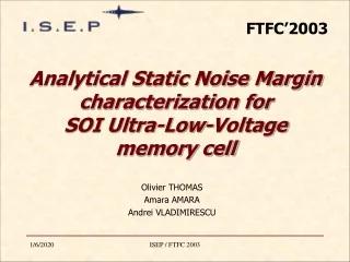
FTFC’2003 Analytical Static Noise Margin characterization for SOI Ultra-Low-Voltagememory cell Olivier THOMAS Amara AMARA Andrei VLADIMIRESCU ISEP / FTFC 2003
Outline • Motivations • Static noise disturbance • Static noise margin (SNM) characterization • Electrical analytic model • Analytic estimation method of the stability • Stability analysis on a 4T Self-Refresh and a 6T full CMOS SRAM cell • Conclusions ISEP / FTFC 2003
Motivations • The emergence of portable or mobile computing and communication devices is the most important factor driving the need for low power design. • The commercial success of such a product depends on the battery life. • Some niche applications do not necessarily need high performance. Operation in Ultra-Low-Voltage is very attractive for achieving significant energy saving. ISEP / FTFC 2003
Outline • Motivations • Static noise disturbance • Static noise margin (SNM) characterization • Electrical analytic model • Analytic estimation method of the stability • Stability analysis on a 4T Self-Refresh and a 6T full CMOS SRAM cell • Conclusions ISEP / FTFC 2003
Static noise disturbance presents in logic gates • Cell stability is influenced by offsets and mismatches due to processing and variations in operating conditions: • Width and length mismatches • Threshold mismatches (non-uniformity of ion implantation or gate oxide thickness) • Also there are 4 other basic types of noise sources: • Series-voltage noise in interconnection lines between gates • induced by inductive coupling to a current gradient di/dt • Charge coupling to inputs or outputs gates • introduced by capacitive coupling to a voltage gradient dV/dt • Ground and power-supply linesvoltage noise • caused by ringing, spikes, voltage drops due to series resistances, etc. Considered as quasi-static if the interval time in which the gradient is present is long compared with the switching speed of the inverting gates ISEP / FTFC 2003
The variation of the body voltage impacts the threshold voltage. Gate Gate Source Source Drain Drain Body Buried oxide Bulk Bulk MOS/BULK MOS/SOI (SOI: Silicon On Insulator) Drain Drain Drain Gate Bulk Gate Bulk Gate Bulk Body Body Source Source Source SOI Transistors disturbance Good isolation between devices Less junction capacitance DTMOS (Dynamic Threshold MOS) Body Tied to Source ISEP / FTFC 2003
Vgate= 0Vdd Idiode Vsource = 0 Vdrain = Vdd Iii Vdiode Vbody > 0 Io=Is + Iii Is SOI DC characterization in Ultra-Low-Voltage • In U-L-V (VDD VTH): • Iii << due to a weak E @ drain ISEP / FTFC 2003
C versus VGS (VDS=0V) C Accumulation Depletion Inversion CG CD/S-G CG-B VDD Vout VT TL VGS In Out WLON VM TD MA(VBS) 243mV WLOFF VSS Vin SOI TRAN characterization in Ultra-Low-Voltage • VDD close to VT The threshold voltage strongly depends on the coupling capacitance CG-B and CD/S-B. • Voltage transfer characteristic of an Invertor: — I.C. --- VIN 10 --- VIN 01 • Charge couplingto body ISEP / FTFC 2003
Outline • Motivations • Static noise disturbance • Static noise margin (SNM) characterization • Electrical analytic model • Analytic estimation method of the stability • Stability analysis on a 4T Self-Refresh and a 6T full CMOS SRAM cell • Conclusions ISEP / FTFC 2003
B A Vn Vn Static Noise Margin (SNM) characterization • The SNM of a SRAM memory cell is defined as the minimum DC noise voltage (Vn) present at each of the cell storage nodes (A and B) necessary to flip the state of the cell to a wrong state. • The memory cell is more vulnerable during a read access. ISEP / FTFC 2003
SNM characterization criteria overview • Maximum Square betweennormal and mirrored voltage transfer characteristic. • Small-Signal Closed-Loop Gain is Unity. • Jacobianof the Kirchhoff equations is Zero. • Coincidence of Roots of the flip-flop equation. • All of these criteria are equivalent* • The SRAM cell stability studies usually is based on the Maximum Square method * J. LOHSTROH, E. SEEVINCK ISEP / FTFC 2003
y SNMH SNML WL WL x B A BLT BLC V Maximum square method • The SNM is obtained by drawing and mirroring the inverter characteristics and finding the maximum possible square between them. • The SNM value results as the smallest edge value of the two squares. ISEP / FTFC 2003
Outline • Motivations • Static noise disturbance • Static noise margin (SNM) characterization • Electrical analytic model • Analytic estimation method of the stability • Stability analysis on a 4T Self-Refresh and a 6T full CMOS SRAM cell • Conclusions ISEP / FTFC 2003
Pseudo- saturated part VGS and VBS dependencies Pseudo-linear part Body Surface Fitting factor potential parameter Subthreshold analytical model used ISEP, ESSCIRC SEP 02 ISEP / FTFC 2003
VBS for floating-body transistor • The equation was derived by curve fitting: • m1 and m2 are stored in a lookup table for different transistor W. • m is a fitting constant • The dependence of VBS on VGS in DC is not significant: • The resulting error is around 3.5% when m1 and m2 are extrapolated at VGS equal VDD/2 ISEP / FTFC 2003
Outline • Motivations • Static noise disturbance • Static noise margin (SNM) characterization • Electrical analytic model • Analytic estimation method of the stability • Stability analysis on a 4T Self-Refresh and a 6T full CMOS SRAM cell • Conclusions ISEP / FTFC 2003
Analytic estimation method of the stability • The SNM estimator has been developed with MATLAB • Methodology: • In retention mode, the floating body potential of each transistor of the memory cell is computed analytically. • In read mode, the VTC for each half cell is derived taking into account the body potential previously computed. In addition body voltage variation induced by gate-body coupling is added. • Finally the SNM is extracted graphically by considering the maximum possible square between the normal and mirrored transfer characteristic. ISEP / FTFC 2003
Outline • Motivations • Static noise disturbance • Static noise margin (SNM) characterization • Electrical analytic model • Analytic estimation method of the stability • Stability analysis on a 4T Self-Refresh and a 6T full CMOS SRAM cell • Conclusions ISEP / FTFC 2003
Simulation environment • Technology: SOI 0.25µm • VT0N,P close to 0.6v • 0.5 Wp/Wn 0.7 @ |VDS|=VDD; (VBS) • Simulation condition: VDD = 0.4v ISEP / FTFC 2003
WL VDD TL1 TL2 IL1 IL2 TA1 TA2 A B IA2 IA1 BLT BLC 4T Self-Refresh SRAM cell • Designed for Ultra-Low-Voltage • 4T S-R architecture: • 2 FB NMOS access transistors • 2 pDTMOS load transistors • Low leakage current • High drive current ISEP / FTFC 2003
WL=0 VDD TL1 TL2 IL1 IL2 TA1 TA2 A=‘1’ B=‘0’ IA2 IA1 BLT BLC Stability in retention mode • BLT & BLC grounded to VSS • WL maintained at 0V • TL1 is ON • TA1, TA2 & TL2 are OFF • Easy to maintain ‘1’ • IonL1 >> IoffA1 • Level ‘0’ depends on IA2 & IL2 • IoffA2(VBS,VDS) & IoffL2(VDS) • If V(‘0’) [VBS(TA2), VDS(TA2)] and VDS(TL2) • IoffA2 goes exponentialy up and IoffA2 becomes higher than IoffL2 • Self refresh behavior ISEP / FTFC 2003
Stability versus q=WA/WL • Stability depends on the ratio: • The error between the estimated and the simulated curves is less than 3% for a ratio q larger than 1.5 • The higher the ratio q, the better the stability ISEP / FTFC 2003
VTC without coupling VTC & VTC computed T C VTC with coupling VTC simulated (Eldo) Without coupling T VTC simulated (Eldo) C Vout (T), Vin (C) (v) SNM (v) Vout (T), Vin (C) (v) D V = 150mV D V = 250mV q = W /W Vin (T) ; Vout (C) (v) Vin (T) ; Vout (C) (v) A L Stability in read mode • VTC without considering the gate-body coupling • Good fit between simulated and analytical results • VTC with and without considering the gate-body coupling • VTCs are degraded • The SNM is affected deeply by the gate-body coupling • For 250mV variation the SNM is divided by 2 • The higher the ratio q, worse the stability This study shows that the ratio q must be well-balanced versus retention and read mode results ISEP / FTFC 2003
WL VDD TL1 TL2 TA1 TA2 1 0 TD1 TD2 BLT 0 BLC 0 VSS VTCT & VTCc computed VTCT simulated (Eldo) VTCc simulated (Eldo) VTCT Vout (I); Vin (II) VTCc Vin (I); Vout (II) 6T Full CMOS SRAM cell • In retention mode: • BLT & BLC grounded to VSS • WL maintained at 0V • VTCT and VTCC are not symmetrical • In retention: • VSTA2 = 0v VBTA2 < 0v (= -74mV) • VSTA1 = VDD VBTA1 > 0v (= 315mV) • In read mode VBS of TA2 becomes more and more negative as V(B) increases, which preventing the voltage to reach VDD. ISEP / FTFC 2003
VTC without coupling VTC with coupling VTCT Vout (I); Vin (II) VTCC Vin (I); Vout (II) Stability in read mode • VTC with and without considering the gate-body coupling • VTCs are degraded ISEP / FTFC 2003
Outline • Motivations • Static noise disturbance • Static noise margin (SNM) characterization • Electrical analytic model • Analytic estimation method of the stability • Stability analysis on a 4T Self-Refresh and a 6T full CMOS SRAM cell • Conclusions ISEP / FTFC 2003
Conclusions • We have developed a simple analytical method to evaluated the SNM of SRAM SOI memory cell working in subthreshold. • This analytical method is based on a simple analytical subthreshold estimation model. • This study shows the importance of the floating body potential when analyzing the stability of CMOS SOI memory cells. • Gate-to-body coupling for the access transistors adds a new important constraint on the stability when the word-line is activated. • For stability reasons the 6T floating-body memory cell working in subthreshold requires small ratios q=WA/WL and r=WA/WD. • For the 4T S-R cell a good stability is reached for a high ratio q=WA/WL. ISEP / FTFC 2003