VLSI Computers
VLSI Computers. COT 4810 Ken Pritchard 30 Sep 04. Overview. Introduction History Physical Description Design Process Fabrication Process. Introduction. VLSI – V ery L arge S cale I ntegration

VLSI Computers
E N D
Presentation Transcript
VLSI Computers COT 4810 Ken Pritchard 30 Sep 04
Overview Introduction History Physical Description Design Process Fabrication Process
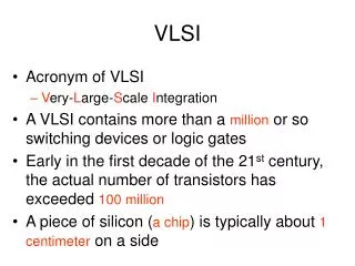
Introduction • VLSI – Very Large Scale Integration • As soon as the transistor was invented, people started trying to combine lots of them together on a single chip. • VLSI is a physical model of integrating many discrete components on a single chip. • VLSI is a design methodology for manufacturing integrated circuits with as many components as possible.
History • First generation computers were assembled with many discrete components, including relays, capacitors, and vacuum tubes. • Second generation computers replaced tubes with transistors. • Third generation computers put many transistors on an integrated circuit or microchip.
Integration History • 1959 – Single Transistor • 1960 – Unit Logic • 1964 – Small Scale Integration with 20 logic units per chip • 1967 – Medium Scale Integration with 200 logic units per chip • 1972 – Large Scale Integration with 2,000 logic units per chip • 1978 – Very Large Scale Integration with 29,000 logic units per chip • 2004 – 410,000,000 transistors on a chip
Physical Aspects • VLSI computers use metal-oxide-semiconductor (MOS) technology. • A MOS transistor has three terminals, with the gate terminal controlling flow between the source and the drain. • There are two kinds of transistors classified by whether they conduct when a high or low voltage is placed on their gate. • The nMOS transistor conducts when a logic 1 is placed on its gate. • The pMOS transistor conducts when a logic 0 is placed on its gate.
A layer of metal sits on top of a layer of silicon dioxide which acts like an insulator. It is on top of a layer of the semiconductor silicon. A photographic-like etching process removes the unnecessary metal. The silicon is doped by diffusing with a special element. The area between the diffusion areas is called the channel. Here it is length L. L
The metal gate sits on top of a layer of silicon dioxide which sits on top of the silicon substrate. The two green areas are diffusion areas with an excess of electrons. When a charge is placed on the gate, the electrons in the silicon are pulled up into the channel and a connection is made between the two diffusion areas. Diagram of nMOS Transistor Gate Gate Source Drain Source Drain nMOS Transistor pMOS Transistor
Details • The metal layer has been replaced by polycrystalline silicon, or polysilicon, but the name MOS survives. • Diffusing the silicon introduces impurities that alter the behavior of the material. • Diffusing with arsenic and phosphorus leaves extra electrons, while boron removes electrons to form “holes” of positive charge. • The length of the channel in an nMOS transistor is inversely proportional to the switching speed. • An nMOS transistor is good at passing logic 0 and not so good at passing logic 1. The opposite is true for a pMOS transistor. Combining the best of both, they are connected to form CMOS, or complimentary metal-oxide-semiconductor, units.
C +5 V GND ~C
Creating a VLSI Circuit • Logic design and layout • Modeling • Simulation • Testing • Fabrication • Not a strict ordering. May have to go from one back to another.
Design The design problem is organized into distinct hierarchical layers that can be optimized. • Partitioning – Divides the circuit into smaller circuits that are more manageable. • Floor Planning – Determines the approximate location of each module in a chip area. • Placement – Decides exactly where modules will be placed and determines wire lengths. • Global Routing – Decomposes overall routing into separate detailed routing problems. • Detailed Routing – Decides actual wire routing taking into consideration horizontal and vertical paths. • Layout Optimization – After layout is finished, see if it can be improved. • Layout Verification – Make sure that it can be built.
Design Continued • There is usually a cooperation between the silicon foundry, the IC design team, and the CAD tool provider during the design and build process. • CAD tools are used throughout the process for design and verification. • Makes use of pre-optimized SSI or MSI cell libraries. • There are various algorithmic techniques employed to optimize the layout process.
Layout Algorithms • Exhaustive Search – Try every possibility and pick the best one. Not realistic when working with n = 100,000,000. • Greedy – Greedy algorithms are often used with optimizations, not always successfully. • Dynamic – The problem is broken into sub-problems recursively and then combined from the bottom up. Used when the sub-problems are related. • Hierarchical – Break the problem into unrelated sub-problems and solve each one. • Genetic Algorithms – Grow a population of pre-optimized cells into the final design. • GA seems to be getting a lot of attention.
Design Styles • Field Programmable Gate Array • All programming is done by the user and turn around time is fast. Not all of the switches can be used. Programming is valid as long as the chip is powered on or until it is programmed again. • Gate Array • Similar to FPGA except that programming is done in manufacturing with masks. Again, not all the switches can be used. Programming is persistent. • Standard-Cells • Custom design built with logic cells stored in standard cell libraries. Requires CAD tools to accomplish the layout and many custom masks for fabrication. All switches are employed. • Full Custom • The entire design is done with CAD tools and custom masks without pre-designed cell libraries. This is becoming very expensive, so there are processes being developed to reuse parts of custom designs in later projects.
Fabrication • Integrated circuits are composed of layers • Each layer is essentially completed before the next is added. • The patterns on the layers are created by a process called lithography which uses masks. • Each layer uses its own mask. • As each layer is built on the previous, a coating of photo-resistant material is applied. The masking process covers the part of the material that is to be kept so that it is not exposed to UV light. • The part of the photo-resistant material that was exposed can now be removed with a solvent. • The exposed layer can be etched with a chemical process. • The remaining photo-resistant material can now be removed with another solvent.
Relationship to Performance • The channel length L is inversely proportional to the switching speed of a transistor. • The smallest possible channel length will produce the fastest speed. • Generally the channel length L is the same as the smallest wire that the fabrication process can produce. • Intel is currently using 90nm technology. • Intel is planning on 65nm technology in 2005.
Summary • Originally, computers were composed of a large number of discrete parts that consumed a lot of power and took up a lot of space. • VLSI computers use a material that is not a conductor or an insulator called a semiconductor. The properties of the semiconductor are modified so that it forms part of an electronically controlled switch. This is called metal-oxide-semiconductor technology. • The MOS components are combined to form logic units and then wired together. Then, as a unit, they perform the functions that had been performed by many discrete parts. • VLSI designs are composed of different layers that are etched or diffused by using masks. • VLSI design has led to a very high density of logic components that use comparatively little power. • The number of transistors on a logic chip is roughly doubling every two years. • Almost any device can be fitted with a VLSI logic and memory device. • Advances in VLSI lead to faster systems which lead to advances in VLSI.
References Katz, Randy A. Contemporary Logic Design. Redwood City: The Benjamin/Cummings Publishing Company, Inc, 1994 Vai, M. Michael VLSI Design. Boca Raton: CRC Press LLC, 2001 Sarrafzadeh, M. and C. K. Wong An Introduction to VLSI Physical Design. Portland: McGraw-Hill, 1996 Dewdney, A. K. The New Turing Omnibus. New York: Henry Holt and Company, 2001 http://developer.intel.com/ http://encyclopedia.thefreedictionary.com/VLSI http://lsiwww.epfl.ch/LSI2001/teaching/webcourse/