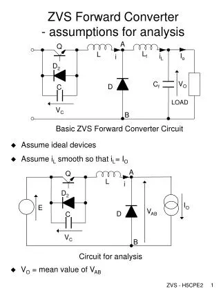
ZVS Forward Converter - assumptions for analysis
90 likes | 314 Vues
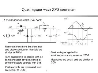
A. Q. L f. L. I o. i L. i. D 2. V O. C f. D. C. LOAD. V C. B. Basic ZVS Forward Converter Circuit. A. Q. L. i. D 2. I O. E. V AB. D. C. V C. B. Circuit for analysis. ZVS Forward Converter - assumptions for analysis. Assume ideal devices

ZVS Forward Converter - assumptions for analysis
E N D
Presentation Transcript
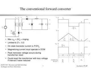
A Q Lf L Io iL i D2 VO Cf D C LOAD VC B Basic ZVS Forward Converter Circuit A Q L i D2 IO E VAB D C VC B Circuit for analysis ZVS Forward Converter- assumptions for analysis • Assume ideal devices • Assume iL smooth so that iL= IO • VO = mean value of VAB
A L i IO E VAB C VC B Equivalent Circuit for Mode 1 ZVS Forward ConverterMode 1 • Before Mode 1 starts Q has been on for some time (see Mode 5) • Mode 1 starts when Q is turned OFF • Conditions at start of Mode 1: VC = 0, i = IO • IO charges C linearly VC rises linearly • VAB = E – VC when VC reaches E, VAB tries to go negative and D turns ON this ends MODE 1 • Duration for Mode 1 is given by:
A L i IO E D VAB C VC B Equivalent Circuit for Mode 2 ZVS Forward ConverterMode 2 • Conditions at start of Mode 2: VC = E, i = IO, D is ON • L and C form a resonant circuit (see separate analysis sheet) • VAB = 0, VC follows an offset sine, i follows a cosine:
A L i IO E D VAB C VC B Equivalent Circuit for Mode 2 ZVS Forward ConverterMode 2 continued D2 • Mode 2 finishes when VC tries to go negative and D2 turns ON • Duration for Mode 2 (2) can be found from: • Value of i (=I’) at the end of Mode 2 is given by: • I’ is negative
A Q L i D2 IO E D VAB C VC B Equivalent Circuit for Mode 3 ZVS Forward ConverterMode 3 • Conditions at start of Mode 3: VC = 0, i = I’ (negative), D is ON, D2 is ON • Resonance stops since C is shorted by D2 • VAB = 0, VC = 0 • Voltage across L = E i increases linearly (towards 0) • Q has a drive (Gate) signal applied during Mode 3, but doesn’t conduct immediately since i is negative • Mode 3 finishes when i reaches 0 and Q takes over i from D2 • Duration for Mode 3 is given by:
A Q L i IO E D VAB C VC B Equivalent Circuit for Mode 4 ZVS Forward ConverterMode 4 • Mode 4 starts when Q takes over i from D2 as it passes through 0 • Conditions at start of Mode 4: VC = 0, i = 0, D is ON, Q is ON • No resonance since C is shorted by Q • VAB = 0, VC = 0 • Voltage across L = E i increases linearly (towards IO) • Mode 4 finishes when i reaches IO and all of the load current is now flowing through Q D turns OFF • Duration for Mode 4 is given by:
A Q L i IO E VAB C VC B Equivalent Circuit for Mode 5 ZVS Forward ConverterMode 5 • Mode 5 starts when D turns OFF since Q has all the load current • Conditions at start of Mode 5: VC = 0, i = IO, D is OFF, Q is ON, D2 is OFF • No resonance since C is shorted by Q • Circuit is in steady state: VAB = E, VC = 0, i = IO • Mode 5 finishes when Q is turned OFF by the control circuit back to Mode 1 • Duration for Mode 5 is controllable and provides the means for controlling the output voltage Vo (= mean value of VAB)