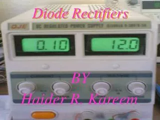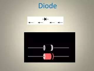
SCHOTTKY BARRIER DIODE
SCHOTTKY BARRIER DIODE. The Schottky diode (named after German physicist Walter H. Schottky; also known as hot carrier diode) is a semiconductor diode with a low forward voltage drop and a very fast switching action.

SCHOTTKY BARRIER DIODE
E N D
Presentation Transcript
SCHOTTKY BARRIER DIODE The Schottky diode (named after German physicist Walter H. Schottky; also known as hot carrier diode) is a semiconductor diode with a low forward voltage drop and a very fast switching action. When current flows through a diode there is a small voltage drop across the diode terminals. A normal silicon diode has a voltage drop between 0.6–1.7 volts, while a Schottky diode voltage drop is between approximately 0.15–0.45 volts. This lower voltage drop can provide higher switching speed and better system efficiency.
CONSTRUCTION • A metal–semiconductor junction is formed between a metal and a semiconductor, creating a Schottky barrier (instead of a semiconductor–semiconductor junction as in conventional diodes). • Typical metals used are molybdenum, platinum, chromium or tungsten; and the semiconductor would typically be N-type silicon. • The metal side acts as the anode and N-type semiconductor acts as the cathode of the diode. This Schottky barrier results in both very fast switching and low forward voltage drop.
Reverse recovery time • The most important difference between the p-n and Schottky diode is reverse recovery time, when the diode switches from conducting to non-conducting state. Where in a p-n diode the reverse recovery time can be in the order of hundreds of nanoseconds and less than 100 ns for fast diodes, Schottky diodes do not have a recovery time, as there is nothing to recover from (i.e. no charge carrier depletion region at the junction). • The switching time is ~100 ps for the small signal diodes, and up to tens of nanoseconds for special high-capacity power diodes. With p-n junction switching, there is also a reverse recovery current, which in high-power semiconductors brings increased EMI noise. With Schottky diodes switching essentially instantly with only slight capacitive loading, this is much less of a concern.
CONSTRUCTION AND APPLICATIONS • It is often said that the Schottky diode is a "majority carrier" semiconductor device. This means that if the semiconductor body is doped n-type, only the n-type carriers (mobile electrons) play a significant role in normal operation of the device. The majority carriers are quickly injected into the conduction band of the metal contact on the other side of the diode to become free moving electrons. Therefore no slow, random recombination of n- and p- type carriers is involved, so that this diode can cease conduction faster than an ordinary p-n rectifier diode. This property in turn allows a smaller device area, which also makes for a faster transition.
This is another reason why Schottky diodes are useful in switch-mode power converters; the high speed of the diode means that the circuit can operate at frequencies in the range 200 kHz to 2 MHz, allowing the use of small inductors and capacitors with greater efficiency than would be possible with other diode types. Small-area Schottky diodes are the heart of RF detectors and mixers, which often operate up to 50 GHz.
Limitations • The most evident limitations of Schottky diodes are the relatively low reverse voltage ratings for silicon-metal Schottky diodes, typically 50 V and below, and a relatively high reverse leakage current. Some higher-voltage designs are available; 200V is considered a high reverse voltage. • Reverse leakage current, because it increases with temperature, leads to a thermal instability issue. This often limits the useful reverse voltage to well below the actual rating. • While higher reverse voltages are achievable, they would be accompanied by higher forward voltage drops, comparable to other types; such a Schottky diode would have no advantage
Applications • Voltage clamping • Reverse current and discharge protection • Power supply
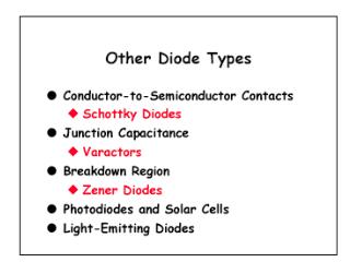
Two-Terminal Devices Having A Single p-n Junction Schottky Tunnel Varactor Photodiode Solar Cell
Other Two-Terminal DevicesOf A Different Construction Photoconductive Cell LCD (Liquid-Crystal Display) Thermistor
Schottky-Barrier Diode *Surface-Barrier/Hot-Carrier Diode
Schottky-Barrier Diode Areas of Application Very high frequency range Lower noise figure Low-voltage or high-current power supplies AC-to-DC converters Radar systems Schottky TTL logic
Gold leaf metal contact Fig. 20.1 Passivated hot-carrier diode Anode (+) Metal Silicon dioxide screen Metal semiconductor junction Metal contact Cathode (-)
ID Fig. 20.2 Comparison of characteristics of hot-carrier and p-n junction diodes Hot carrier diode p-n junction diode VD p-n junction diode Hot carrier diode
Fig. 20.3 Schottky (hot-carrier) diode: (a) equivalent circuit; (b) symbol (a)
Fig. 20.4 Approximate equivalent circuit for the Schottky diode
Fig. 20.5 Motorola Schottky barrier devices.(Courtesy Motorola Semiconductor Products, Incorporated
Fig 20.6 Characteristics curves for Hewlett-Packard 5082-2300 series of general-purpose Schottky barrier diodes. 100 10 Forward current (mA) IF Temperature Coeffiecient 10A -2.3mV/ºC 100A -1.8mV/ºC 1.0mA -1.3mV/ºC 10mA -0.7mV/ºC 100mA -0.2mV/ºC 1 .1 T = 100ºC T = 25ºC T = -50ºC 0.1 0 100 200 300 400 500 600 700 Forward voltage (mV) I-V Curve Showing Typical Temperature Variation for 5082-2300 Series Schottky Diodes (a)
100 500 Reverse current (nA) 2900 2303 100 50 2301 2302 2305 10 0 5 10 15 Reverse voltage (V) 5082-2300 Series Typical Reverse Current vs. Reverse Voltage at TA = 25ºC (b)
1.2 1.0 0.8 Capacitance (pF) 0.6 2900 2303 0.3 2301 2302 2305 0.2 0 4 8 12 16 20 VR-Reverse voltage (V) 5082-2300 Series Typical Capacitance vs. Reverse Voltage at TA = 25ºC (c)
Schottky diode I-V characteristics Schottky diode is a metal-semiconductor (MS) diode Historically, Schottky diodes are the oldest diodes MS diode electrostatics and the general shape of the MS diode I-V characteristics are similar to p+n diodes, but the details of current flow are different. Dominant currents in a p+n diode • arise from recombination in the depletion layer under small forward bias. • arise from hole injection from p+ side under larger forward bias. Dominant currents in a MS Schottky diodes • Electron injection from the semiconductor to the metal.
Current components in a p+n and MS Schottky diodes M n-Si p+ n dominant negligible B Ir-g IR-G negligible dominant
I-V characteristics where B is Schottky barrier height, VA is applied voltage, A is area, and A* is Richardson’s constant. The reverse leakage current for a Schottky diode is generally much larger than that for a p+n diode. Since MS Schottky diode is a majority carrier devices, the frequency response of the device is much higher than that of equivalent p+ n diode.