Download
1 / 3
40 likes | 210 Vues
Nanoscale Schottky Barrier Measured Using STM.

E N D
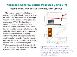
Nanoscale Schottky Barrier Measured Using STM The current-voltage (I-V) behavior of nanoscale metallic islands epitaxially grown on Si(111) has been measured in ultrahigh vacuum (UHV) using a scanning tunneling microscope (STM). The islands are atomically perfect, with well-defined interface, surface and corner facets. Thus, they are ideal for testing the behavior of the Schottky Barrier for nanoscale structures. It is found that tunneling is markedly enhanced due to field concentration at the small metallic electrode. Thus the current becomes particularly sensitive to the shape of the island, as shown in the figure. Understanding and control of such effects will be necessary for many semiconductor-based nanoelectronic devices. Peter Bennett, Arizona State University, DMR 0503705 Top: Comparison of I-V for nanoscale vs. conventional Schottky diode. Inset shows a cross-section TEM image of an epitaxial CoSi2 island on Si(111). Bottom: I-V curves for differently shaped islands.
Nanowire Resistivity Much attention has focused lately on the use of nanowires (NWs) for nanoelectronic applications, particularly semiconducting NWs, which can be gated to form a field effect transistor. Here we show self-assembled silicide NWs epitaxially grown on silicon, which have potential application as interconnects between active elements. Such NWs are smaller (a few nm) and better (perfect single crystal) than what can be made using electron-beam lithography. It is found that the resistivity of the NW increases sharply as the NW dimension shrinks below 50 nm. These effects are not well understood at present, but will have to be controlled for future applications. Peter Bennett, Arizona State University, DMR-0503705 Top: SEM image of two STM probes contacting a nanowire. Bottom: Resistance vs probe spacing, from which resistivity and contact resistance may be obtained directly. H. Okino, I. Matsuda, P. A. Bennett, and S. Hasegawa, App. Phys. Lett. 86, 233108 (2005).
Peter Bennett, Arizona State University, DMR-0503705 Students in the Freshman physics lab measure the resistivity of a graphite rod, by measuring R vs probe separation, precisely analogous to the NW experiments using STM. The application of simple concept into the “World of Nano” in a contemporary experiment, brings a special excitement and context to the project.