Download
1 / 40
400 likes | 427 Vues
Explore the fundamentals of analog and digital design, focusing on non-linear elements, active elements like MOSFETs and operational amplifiers. Get insights into pn-junction diodes, ideal diode modeling, and MOSFET amplification principles in this comprehensive lecture material. Learn about circuit analyses for non-linear elements and practical applications in electronic circuits. Dive into the world of semiconductor devices and understand the characteristics of pn-junction diodes and MOSFET transistors. Enhance your knowledge with real-world examples and laboratory exercises in analog and digital electronic circuits.

E N D
Fundamentals of Analog and Digital Design ET-IDA-134 Lecture-04 Non-linear Elements, Active Elements MOSFETS Operational Amplifiers 11.12.2018, v13 Prof. W. Adi Source: Analog Devices, Digilent course material
Agarwal, Anant, and Jeffrey H. Lang. Foundationsof Analog and Digital Electronic Circuits. San Mateo, CA: Morgan Kaufmann Publishers, Elsevier, July 2005. ISBN: 9781558607354.View e-book versionElsevier companion site: supplementary sections and examples Course Contents Lecture Material: Recommended Textbook: - Provided in theclass. Source: Digilent/Analog Devices Course material - Suplimentaryadvanced analog and digital design topicswithlaboratory Laboratory: - Digilent Analog Discovery withlab‘skit. Web Digilent material Link: http://www.digilentinc.com/Classroom/RealAnalog/
PN-Diode Water Model for a Diode rectifier pn-Diode (Symbol) Water model for a pn-Diode
The pn-Junction Diode Circuit Symbol Schematic description ID Anode Cathode p-doped n-doped + UD– Acceptors- Concentration NA Donators- Concentration ND ID + UD – metal SiO2 SiO2 Physical Structure: (Example) p-type Si n-type Si metal
Summary of a : pn-Junction Diode I-U Characteristics • In conducting direction: The diode current ID grows exponentially with the forward voltage UD. Where UT = K T /q ≈ 26 mV, m= 1.. 2 (correction factor) (K: Boltzmann Constante = 1,38 · 10-23 VAs/K , q: Electron Charge= 1,602 · 10-19 As, T: Temperature in Kelvin = 273 + Temperature in C) • In reverse mode (isolation mode) a very low current IS ≈ 1 nA (Si) flows through the diode [ISis temperature dependent( Exp.). ID (A) The result is the following I, U curve having very low current for UD <0 and high current (conducting) for UD >0 UD (V) 0.7 V für Si IS ≈ 1 nA (Si) Threshold voltage
The Ideal Diode: Modell for the pn-Diode I-U Curve As switch Circuit Symbol ID ID (A) + UD – ID UD Backward Direction Forward Direction UD (V) • An ideal diode allows current flow only in one direction. • An Ideal Diodehas the following properties:: • If ID > 0, UD = 0 • If UD < 0, ID = 0 • Diode operates as a switch: • Closed in forward direction • Open in backward direction
Large Signal Diode Model I-U Curve As switch Circuit Symbol ID ID (A) ID + UD – + UD – Uon Forward Direction Backward Direction UD (V) Uon For Si pn Diode, Uon 0.7 V Rule 1: If ID > 0, UD = Uon. Rule 2: If UD < Uon., ID = 0
pn-Junction Backwards Breakdown • I the reverse voltage exceeds a critical value, (Ecrit 2x10⁵ V/cm), Then the backward current increases dramatically and destroys the junction. ID (A) Backwards diffusion current Forward current UBD Breakdown Voltage UD (V)
Circuit Analysis for non-linear Elements As the pn-junction is a non-linear element, the circuit analysis becomes more complicated!! (Node and Mesh equations do not work as before) Mesh-Equation: UTh = RTh ID + UD => ID = - (1/ RTh ) UD +UTh/RTh(1) (2) ID RTh + UD Solve two equations with two unknowns! UTh The result is a non-linear equation with one unknown: - (1/ RTh ) UD +UTh/RTh = Hard to solve! Therefore a graphical solution!
Graphical “Load Line“ Solution • Draw I-U relationship for the non-linear element and for the rest of the circuit • The operation point (or the solution of both equations) is the intersection point between the two curves. I ID + UD – RTh UTh/RTh Operation point (intersection point) UTh ID U UD UTh The I-U relationship of the whole circuit without the non-linear element is called the „Load Line“. ID = - (1/ RTh ) UD +UTh/RTh
MOSFET Amplification Principle Drain Basic principle of a MOSFET amplifier: The drain current flow IDis controlled by the electrical field of the gate . ID is also proportional to the gate voltage UG. Amplification: a low voltage change on the gate produces large current changes between drain and source. ID E Gate E UG Source Mechanical Model See . Gate Drain Source
MOSFET Transistor Types NMOS G G G S D n+ poly-Si n+ n+ S S p-doped Si Substrate G PMOS G G S D p+ poly-Si S S p+ p+ n-doped Si Substrate
For small UDS : MOSFET is seen as a controlled resistor • A MOSFET acts as a resistor for small UDS: • That is drain current ID grows linearly with UDS • The resistance RDS between SOURCE & DRAIN depends on UGS - RDS becomes smaller when UGS is more than UT This operation mode is very important for digital circuits ! NMOSFET example: UDS UGS ID UGS = 2 V UGS = 1 V > UT UGS< UT UDS IDS = 0 if UGS< UT
Summary of ID ,UDS characteristic line • The MOSFET ID-UDS curve has two regions:: • 1) the Ohmic or “Trioden- region : 0 < UDS < UGS UT • 2) The Saturation region: UDS > UGS UT D ID G UDS UGS S UGS= 2.5 V UDS = UGS UT ID (A) Ohmic „Trioden“ region saturation ProzessTranskonductance Parameter UGS= 2.0 V UGS= 1.5 V UGS= 1.0 V UDS (V) IDSAT= f(UGS) = constant “CUTOFF” Region: UG < UT
Measuring UT for a MOSFET • UT can be quantified by measuring ID as a function of UGS for small values of UDS ( UDS << UGS-UT) : ID (A) UGS (V) for UGS = UT , : ID ≈ 0 0 UT
MOSFET as an Ohmic Switch • For digital circuits, a MOSFET is either in cut-off „OFF“ (UGS < UT) or in conducting „ON“ (UGS = UDD) condition. We need to consider only two regions in the ID , UDS curve: • Region where UGS < UT • Region for UGS = UDD (UDD :supply voltage) D ID UGS = UDD (on-condition) Req ID UGS UGS >UT VDS UGS< UT(off-condition) S
The Equivalent Resistor Req • In digital circuits an n-channel MOSFET is used to discharge a load capacity Cload under the following condition: • Gate- voltage UG = UDD • Source voltage US = 0 V • Drain voltage UD with initial value UDD, discharged by drain current to 0 The value of Reqis selected to attain the required delay time td. (td is often considered as the time required to reach ½ UDD ): UDSdischarging from UDD UDD/2 UDD UDD Clast ID Cload Req
Typical MOSFET Parameters • A sample MOSFET parameters: • UT (~0.5 V) • Coxand k (<0.001 A/V2) • UDSAT ( 1 V) • l ( 0.1 V-1) ExampleReqvalue for 0.25 mm Technology (W = L): UDD (V)
iD uDS 0 How does a MOSFET Transistor amplify? Amplifying the input signal us UDD RD uDS= uGS–UT UDSAT iD us “LINEAR” orr “TRIODE” UDD RD + UOut= uDS + “Saturation” + uGS + – UBIAS uGS=UBIAS + US Input signal at gate uGS = UBIAS + us uGS=UBIAS uGS uGS=UBIAS -US UDD UOut= uDS Operating point Output Voltage Swing Range
Input Signal and bias for a linear amplifier UDD us UDD = ID RD +uOut + uGS + – UBIAS RD ID R1 UBIAS = UDD R2/(R1+R2) UBIAS uOut R2 us uGS UBIAS: DC voltage component uGS uS : Changing voltage component uGS
MOSFET When discharging UDS goes from UDD to 0 V slope UDD / IDSAT MOSFET switches on (UGS = UDD) and UDS = UDD slope UDD / 2 IDSAT NMOSFET Summary: Digital Circuit Model • For digital circuits a MMOSFET is modeled as a switched resistor Change from 1 to 0: UDSDischarged from UDD UDD/2 UGS > UT Req UGS = UDD S D Clast Clast ID Req UGS = 0 iD UGS = UDD= “1” IDSAT UGS = 0 UDS 0 UDD/2 UDD • UDS =“0” • UDS =“1”
B C-MOSFET (Complementary Symmetric ) Digital Switch On for 1 P-MOS B B Req-P B N-MOS Req-N On for 0
UDD S G D UA UE D G S CMOS Inverter: model and operating points Circuit Switch modelsforbothestates UDD UDD Rp Low UAL = 0 V High UAH = UDD UA UA Rn Low energy consumption as no current flow in both low and high states UE = UDD UE = 0 V
CMOS Inverter: Models and operationpoints Switch modelforlowoutput UA=0 and high output UA=UDD UDD UDD Rp UA-high = UDD UA UA CL UA-low = 0 V CL Rn UDD UDD UA UA UE = 0 V UE = UDD tpHL tpLH
Example : C-MOS Circuit and switching speed computation • Set up the truth table of the function F(A,B,C) • Implement the function in C-MOS transistors • Compute the maximum and minimum (best-case and worst case) possible operating speed of the function F. Assume that the switching resistance for P-MOS transistor is RP=7 kΩand for N-MOS transistor RN=5kΩ and the load capacitor is 3 pF. Solution: 1. From the truth table: 2. By Boolean reduction/manipulation and reorganization/minimization of the function: (notice other solutions are possible):
B B B UDD A B C A F C B A B C USSD
B B B Worst case Best case UDD UDD 5. Any switching to high=1 state involves two P transistors in series UDD 7kΩ 7kΩ A 7kΩ 7kΩ T1 Any switching to low=0 state involves on of the two cases B C 5kΩ 5kΩ UA UA T2 c=3pF c=3pF F 5kΩ 5kΩ 5kΩ tpLH=0.69 RpC = 0,69 (7+7)kΩ x 3pF tpLH= 29 ns B A CL Best case: tpHL=0.69 RnC = 0,69 (5+2,5)kΩ x 3pF tpHL= 15,5 ns T3 B Worst case: tpHL=0.69 RnC = 0,69 (5+10)kΩ x 3pF tpHL= 31,05 ns C T5 T4 USSD Maximum operating frequency FMax= 1/2(tpHL+ tpLH) =1/2(29+15,n)ns = 11,24 MHz Minimum operating frequency FMax= 1/2(tpHL+ tpLH) =1/2(29+31,05)ns = 8,33 MHz
Operational Amplifiers • So far, with the exception of our ideal power sources, all the circuit elements we have examined have been passive • Total energy delivered by the circuit to the element is non-negative • We now introduce another class of active devices • Operational Amplifiers (op-amps) • Note: These require an external power supply!
Operational Amplifiers – overview • We will analyze op-amps as a “device” or “black box”, without worrying about their internal circuitry • This may make it appear as if KVL, KCL do not apply to the operational amplifier • Our analysis is based on “rules” for the overall op-amp operation, and not performing a detailed analysis of the internal circuitry • We want to use op-amps to perform operations, not design and build the op-amps themselves
Amplifire Abstraction Abstract description Amplifire principle UDD UDD A RD ID uin uout uout= A . uin uout Or simply: uin A uout= A . uin uin A = uout/uinas Amplification factor
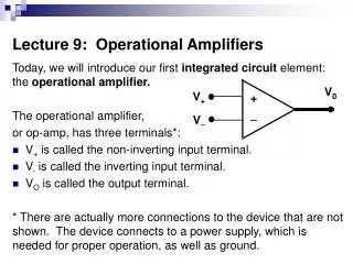
Full-Operational Amplifire Abstraction Amplifies the difference between u1 and u2 ! +UB Abstraction Symbol u+ + - + - uA u- u+ u- uA= A . ( u+ – u- ) -UB Op-Amp equivalent circuit • IdealOperational Amplifire: • Has 2 inputs (negative - and positive +) and one output • Where: • Input resistance Ri=> ∞ • Output resistance Ro => 0 • Amplification factor A => ∞ + - u+ Ro u=u+–u- Ri uA A . u u-
8 V 8 μV uA= A . u = 106 x 8 μV = 8 V Characteristic Response of an operational amplifier Op-Amp equivalent circuit Abstract Symbol +12V + - u+ u+ + - u=u+–u- uA uA = A u A . u u- u- -12V uA • Example • Input resistance Ri= 10 MΩ • output resistance Ro = 10 Ω • Amplification factor A = 106=> ∞ Saturation +12V u Linear active region A is very high Temperature dependent! -12V Saturation
Ideal Operational Amplifier “Rules” • More complete circuit symbol • (Power supplies shown) • Assumptions: • ip = 0, in = 0 • vin = 0 • V - < vout < V +
Operational Amplifire with Feedback1- (Non-Inverting Mode) Op-Amp equiv. circuit analysis R1 R2 R1 R2 uA U- u- - + uE=u+ u- u=u+–u- uA=A(u+–u-) A . u uE=u+ How is the relationship between uA and uE? uA = A (u+ - u-) Rein=∞ Amplification factor in feedback mode uA/uEis independent on A!
Op-amp circuit – Non-Inverting Mode • Find Vout 0 A 0 V i 0 A Rin i
Operational Amplifire with Feedback1-(Non-Inverting Buffer) R1 R2 uA U- - + uE=u+ (Special case: Buffer Amplifire) Called Buffer amplifire: Amplification factor uA/uE= 1 Input resistance Rein=∞ Output resistance RAusg= 0 Current amplification = ∞ - + uA = uE uE
Operational Amplifire with Feedback2- (Inverting Mode) Op-Amp equivalent circuit R1 uE R2 R1 R2 uE u- uA u- - + u+=0 u- u=u+–u- uA=A(u+–u-) A . u u+=0 How is the relationship between uA and uE? uA = A (u+ - u-) Rin= R1 Amplification factor in feedback mode uA/uEis independent on A!
Op-amp circuit – Inverting-Mode • Find Vout i -i 0 A 0 V
Examples: Operational Amplifire with Feedback 1- Inverting Mode: uE R1= 1 kΩ R2= 15 kΩ uA - + Rin= R1= 1 kΩ 2- Non-Inverting Mode: R2= 9 kΩ R1= 1 kΩ uA - + uE Rin=∞