Chapter 3 Bipolar Junction Transistor (BJT)
930 likes | 1.37k Vues
Chapter 3 Bipolar Junction Transistor (BJT). Outline. Introduction Operation in the Active Mode Analysis of Transistor Circuits at DC The transistor as an Amplifier Graphical Analysis Biasing the BJT for Discrete-Circuit Design Configuration for Basic Single Stage BJT Amplifier

Chapter 3 Bipolar Junction Transistor (BJT)
E N D
Presentation Transcript
Chapter 3 Bipolar Junction Transistor (BJT) SJTU Zhou Lingling
Outline • Introduction • Operation in the Active Mode • Analysis of Transistor Circuits at DC • The transistor as an Amplifier • Graphical Analysis • Biasing the BJT for Discrete-Circuit Design • Configuration for Basic Single Stage BJT Amplifier • High frequency Model SJTU Zhou Lingling
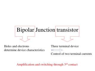
Introduction • Physical Structure • Circuit Symbols for BJTs • Modes of Operation • Basic Characteristic SJTU Zhou Lingling
Physical Structure A simplified structure of the npn transistor. SJTU Zhou Lingling
Physical Structure A dual of the npn is called pnp type. This is the simplified structure of the pnp transistor. SJTU Zhou Lingling
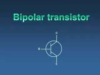
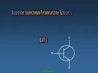
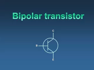
Circuit Symbols for BJTs The emitter is distinguished by the arrowhead. SJTU Zhou Lingling
Modes EBJ CBJ Application Cutoff Reverse Reverse Switching application in digital circuits Saturation Forward Forward Active Forward Reverse Amplifier Reverse active Reverse Forward Performance degradation Modes of Operation SJTU Zhou Lingling
Basic Characteristics • Far more useful than two terminal devices (such as diodes) • The voltage between two terminals can control the current flowing in the third terminal. We can say that the collector current can be controlled by the voltage across EB junction. • Much popular application is to be an amplifier SJTU Zhou Lingling
Operation in the Active Mode • Current flow • Current equation • Graphical representation of transistor’s characteristics SJTU Zhou Lingling
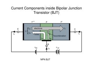
Current Flow Current flow in an npn transistor biased to operate in the active mode. SJTU Zhou Lingling
Collector Current • Collector current is the drift current. • Carriers are successful excess minority carriers. • The magnitude of collector current is almost independent of voltage across CB junction. • This current can be calculated by the gradient of the profile of electron concentration in base region. SJTU Zhou Lingling
Base Current • Base current consists of two components. • Diffusion current • Recombination current • Recombination current is dominant. • The value of base current is very small. SJTU Zhou Lingling
Emitter Current • Emitter current consists of two components. • Both of them are diffusion currents. • Heavily doped in emitter region. • Diffusion current produced by the majority in emitter region is dominant. SJTU Zhou Lingling
Profiles of Minority-Carrier Concentrations SJTU Zhou Lingling
Current Equation • Collector current • Base current • Emitter current SJTU Zhou Lingling
Explanation for Saturation Current • Saturation current is also called current scale. • Expression for saturation current: • Has strong function with temperature due to intrinsic carrier concentration. • Its value is usually in the range of 10-12A to 10-18A. SJTU Zhou Lingling
Explanation for Common-Emitter Current Gain • Expression for common –emitter current gain: • Its value is highly influenced by two factors. • Its value is in the range 50 to 200 for general transistor. SJTU Zhou Lingling
Explanation for Common-Base Current Gain • Expression for common –base current gain: • Its value is less than but very close to unity. • Small changes in α correspond to very large changes in β. SJTU Zhou Lingling
Recapitulation • Collector current has the exponential relationship with forward-biased voltage as long as the CB junction remains reverse-biased. • To behave as an ideal constant current source. • Emitter current is approximately equal to collector current. SJTU Zhou Lingling
Graphical Representation of Transistor’s Characteristics • Characteristic curve relates to a certain configuration. • Input curve is much similar to that of the diode, only output curves are shown here. • Three regions are shown in output curves. • Early Effect is shown in output curve of CE configuration. SJTU Zhou Lingling
Output Curves for CB Configuration SJTU Zhou Lingling
Output Curves for CB Configuration • Active region • EBJ is forward-biased, CBJ is reverse-biased; • Equal distance between neighbouring output curves; • Almost horizontal, but slightly positive slope. • Saturation region • EBJ and CBJ are not only forward-biased but also turned on; • Collector current is diffusion current not drift current. • Turn on voltage for CBJ is smaller than that of EBJ. • Breakdown region • EBJ forward-biased, CBJ reverse-biased; • Great voltage value give rise to CBJ breakdown; • Collector current increases dramatically. SJTU Zhou Lingling
Output Curves for CE Configuration (a) Conceptual circuit for measuring the iC–vCE characteristics of the BJT. (b) The iC–vCE characteristics of a practical BJT. SJTU Zhou Lingling
The Early Effect • Curves in active region are more sloped than those in CB configuration. • Early voltage. • Effective base width and base width modulation. SJTU Zhou Lingling
The Early Effect(cont’d) • Assuming current scale remains constant, collector current is modified by this term: • Narrow base width, small value of Early voltage, strong effect of base width modulation, strong linear dependence of on . SJTU Zhou Lingling
Analysis of Transistor Circuit at DC • Equivalent Circuit Models • Analysis Steps • Examples SJTU Zhou Lingling
Equivalent Circuit Models Large-signal equivalent-circuit models of the npn BJT operating in the forward active mode. In practical DC analysis, constant voltage drop model is popular used. SJTU Zhou Lingling
DC Analysis Steps • Using simple constant-voltage drop model, assuming , irrespective of the exact value of currents. • Assuming the device operates at the active region, we can apply the relationship between IB, IC, and IE, to determine the voltage VCE or VCB. • Check the value of VCE or VCB, if • VC>VB(or VCE>0.2V), the assumption is correct. • VC<VB (or VCE<0.2V), the assumption is incorrect. It means the BJT is operating in saturation region. Thus we shall assume VCE=VCE(sat) to obtain IC. Here the common emitter current gain is defined as forced=IC/IB, we will find forced< . SJTU Zhou Lingling
Examples • Example 5.4 shows the order of the analysis steps indicated by the circled numbers. • Example 5.5 shows the analysis of BJT operating saturation mode. • Example 5.6 shows the transistor operating in cutoff mode. SJTU Zhou Lingling
Examples(cont’d) • Example 5.7 shows the analysis for pnp type circuit. It indicates the the current is affected by ill-specified parameter β. As a rule, one should strive to design the circuit such that its performance is as insensitive to the value of β as possible. • Example 5.8 is the bad design due to the currents critically depending on the value of β. • Example 5.9 is similar to the example 5.5 except the transistor is pnp type. SJTU Zhou Lingling
Examples(cont’d) • Example 5.10 shows the application of Thévenin’s theorem in calculating emitter current and so on. This circuit is the good design for the emitter is almost independent of β and temperature. • Example 5.11 shows the DC analysis for two stage amplifier. • Example 5.12 shows the analysis of the power amplifier composed of the complimentary transistors. SJTU Zhou Lingling
The Transistor as an Amplifier • Conceptual Circuits • Small-signal equivalent circuit models • Application of the small-signal equivalent circuit models • Augmenting the hybrid π model. SJTU Zhou Lingling
Conceptual Circuit (a) Conceptual circuit to illustrate the operation of the transistor as an amplifier. (b) The circuit of (a) with the signal source vbe eliminated for dc (bias) analysis. SJTU Zhou Lingling
Conceptual Circuit(cont’d) With the dc sources (VBE and VCC) eliminated (short circuited), thus only the signal components are present. Note that this is a representation of the signal operation of the BJT and not an actual amplifier circuit. SJTU Zhou Lingling
Small-Signal Circuit Models • Transconductance • Input resistance at base • Input resistance at emitter • Hybrid π and T model SJTU Zhou Lingling
Transconductance • Expression • Physical meaning gm is the slope of the iC–vBE curve at the bias point Q. • At room temperature, SJTU Zhou Lingling
Input Resistance at Base and Emitter • Input resistance at base • Input resistance at emitter • Relationship between these two resistances SJTU Zhou Lingling
The Hybrid- Model • The equivalent circuit in (a) represents the BJT as a voltage-controlled current source (a transconductance amplifier), • The equivalent circuit in (b) represents the BJT as a current-controlled current source (a current amplifier). SJTU Zhou Lingling
The T Model • These models explicitly show the emitter resistance re rather than the base resistance rp featured in the hybrid-p model. SJTU Zhou Lingling
Augmenting the Hybrid- Model • Expression for the output resistance. • Output resistance represents the Early Effect(or base width modulation) SJTU Zhou Lingling
Models for pnp Type • Models derived from npn type transistor apply equally well to pnp transistor with no changes of polarities. Because the small signal can not change the bias conditions, small signal models are independent of polarities. • No matter what the configuration is, model is unique. Which one to be selected is only determined by the simplest analysis. SJTU Zhou Lingling
Graphical Analysis • Graphical construction for the determination of the dc base current in the circuit. • Load line intersects with the input characteristic curve. SJTU Zhou Lingling
Graphical Analysis(cont’d) Graphical construction for determining the dc collector current IC and the collector-to-emitter voltage VCE in the circuit. SJTU Zhou Lingling
Small Signal Analysis Graphical determination of the signal components vbe, ib, ic, and vce when a signal component vi is superimposed on the dc voltage VBB SJTU Zhou Lingling
Effect of Bias-Point Location on Allowable Signal Swing • Load-line A results in bias point QA with a corresponding VCEwhich is too close to VCCand thus limits the positive swing of vCE. • At the other extreme, load-line B results in an operating point too close to the saturation region, thus limiting the negative swing of vCE. SJTU Zhou Lingling
Biasing in BJT Amplifier Circuit • Biasing with voltage • Classical discrete circuit bias arrangement • Single power supply • Two-power-supply • With feedback resistor • Biasing with current source SJTU Zhou Lingling
Classical Discrete Circuit Bias Arrangement • by fixing VBE by fixing IB. SJTU Zhou Lingling
Classical Discrete Circuit Bias Arrangement • Both result in wide variations in IC and hence in VCE and therefore are considered to be “bad.” • Neither scheme is recommended. SJTU Zhou Lingling
Classical Biasing for BJTs Using a Single Power Supply • Circuit with the voltage divider supplying the base replaced with its Thévenin equivalent. • Stabilizing the DC emitter current is obtained by considering the negative feedback action provided by RE SJTU Zhou Lingling
Classical Biasing for BJTs Using a Single Power Supply • Two constraints • Rules of thumb SJTU Zhou Lingling