Download
1 / 20
250 likes | 449 Vues
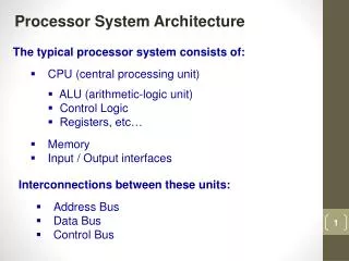
Processor System Architecture. The typical processor system consists of: CPU (central processing unit) ALU (arithmetic-logic unit) Control Logic Registers, etc… Memory Input / Output interfaces. Interconnections between these units: Address Bus Data Bus Control Bus.

E N D
Processor System Architecture The typical processor system consists of: • CPU (central processing unit) • ALU (arithmetic-logic unit) • Control Logic • Registers, etc… • Memory • Input / Output interfaces Interconnections between these units: • Address Bus • Data Bus • Control Bus
Microprocessor :- • It is a programmable digital device, designed with registers, flip-flops, Timing elements which has a set of instructions, designed internally, to manipulate data and communicate with peripherals. • The microprocessor can respond to external signals. It can be interrupted, reset, or asked to wait to synchronize with slower peripherals. Operation Types in a Microprocessor • All of the operations of the microprocessor can be classified into one of three types: • Microprocessor Initiated Operations • Internal Operations • Peripheral Initiated Operations
Microprocessor – Initiated Operations and 8085 BUS Organization • Microprocessor Performs primarily four operations as a part of communication process between MPU and peripheral devices. • Memory Read : Reads data ( instructions) from memory • Memory Write : Writes data ( instructions) in to memory • I/O Read : Accepts data from input devices. • I/O Write : Sends data to output devices • To communicate with a peripheral, the MPU need to perform following steps :- • Identify the peripherals or the memory location (with its address) • Transfer binary information ( data and instructions ) • Provide timing or synchronization signals (control signals)
Bus and CPU Bus: A shared group of wires used for communicating signals among devices • address bus: • the device and the location within the device that is being accessed • data bus: • the data value being communicated • control bus: • describes the action on the address and data buses CPU: Core of the processor, where instructions are executed • High-level language: a = b + c • Assembly language: add r1 r2 r3 • [ • Machine language: 0001001010111010101
The 8085 Bus Structure • The 8-bit 8085 CPU (or MPU – Micro Processing Unit) communicates with the other units using a 16-bit address bus, an 8-bit data bus and a control bus.
The 8085 Bus Structure Address Bus • Consists of 16 address lines: A0 – A15 • Operates in unidirectional mode: • The address bits are always sent from the MPU to peripheral devices in one direction , not reverse. • MPU uses the address bus to perform first function : identifying a peripheral or a memory location • 16 address lines are capable of addressing a Total of 216 = 65,536 (64k) memory locations. • Address locations: 0000 (hex) – FFFF (hex) • When the 8085 wants to access a peripheral or a memory location, it places the 16-bit address on the address bus and then sends the appropriate control signals.
The 8085 Bus Structure Data Bus • Consists of 8 data lines: D0 – D7 • Operates in bidirectional mode: The data bits are sent from the MPU to peripheral devices, as well as from the peripheral devices to the MPU. • The MPU uses the data bus to perform second function : Transfer binary information ( data and instructions ) • Data range: 00 (hex) – FF (hex) Control Bus • Comprised of various single lines that carry synchronization signals. • The MPU uses such lines to perform third function : Provide timing or synchronization signals (control signals)
The 8085: CPU Internal Structure The internal architecture of the 8085 CPU is capable of performing the following operations: • Store 8-bit data (Registers, Accumulator) • Perform arithmetic and logic operations (ALU) • Test for conditions (IF / THEN) • Sequence the execution of instructions • Store temporary data in RAM during execution
The Read Operation • To read the contents of a memory location, the following steps take place: • The microprocessor places the 16-bit address of the memory location on the address bus. • The microprocessor activates a control signal called “memory read” which enables the memory chip. • The memory decodes the address and identifies the right location. • The memory places the contents on the data bus. • The microprocessor reads the value of the data bus after a certain amount of time.
Internal Data Operations • The 8085 can perform a number of internal operations. Such as: storing data, Arithmetic & Logic operations, Testing for condition, etc. • To perform these operations, the microprocessor needs an internal architecture similar to the following:
The Internal Architecture Registers • Six general purpose 8-bit registers: B, C, D, E, H, L • They can also be combined as register pairs to perform 16-bit operations: BC, DE, HL • Registers are programmable (data load, move, etc.) Accumulator • Single 8-bit register that is part of the ALU • Used for arithmetic / logic operations – the result is always stored in the accumulator. Flag Bits • Indicate the result of condition tests. • Carry, Zero, Sign, Parity, etc. • Conditional operations (IF / THEN) are executed based on the condition of these flag bits.
The Internal Architecture • The Program Counter (PC) • This is a register that is used to control the sequencing of the execution of instructions. • This register always holds the address of the next instruction. • Since it holds an address, it must be 16 bits wide. • The Stack pointer • The stack pointer is also a 16-bit register that is used to point into memory. • The memory this register points to is a special area called the stack. • The stack is an area of memory used to hold data that will be retreived soon. • The stack is usually accessed in a Last In First Out (LIFO) fashion.
Externally Initiated Operations • External devices can initiate (start) one of the 4 following operations: • Reset • All operations are stopped and the program counter is reset to 0000. • Interrupt • The microprocessor’s operations are interrupted and the microprocessor executes what is called a “service routine”. • This routine “handles” the interrupt, (perform the necessary operations). Then the microprocessor returns to its previous operations and continues.
Externally Initiated Operations • Ready • The 8085 has a pin called RDY. This pin is used by external devices to stop the 8085 until they catch up. • As long as the RDY pin is low, the 8085 will be in a wait state. • Hold • The 8085 has a pin called HOLD. This pin is used by external devices to gain control of the busses. • When the HOLD signal is activated by an external device, the 8085 stops executing instructions and stops using the busses. • This would allow external devices to control the information on the busses. Example DMA.
The 8085: CPU Internal Structure Simplified block diagram
Example: Instruction Fetch Operation • All instructions (program steps) are stored in memory. • To run a program, the individual instructions must be read from the memory in sequence, and executed. • Program counter puts the 16-bit memory address of the instruction on the address bus • Control unit sends the Memory Read Enable signal to access the memory • The 8-bit instruction stored in memory is placed on the data bus and transferred to the instruction decoder • Instruction is decoded and executed