Download
1 / 11
130 likes | 529 Vues
Characterization of FD-SOI MOSFETs Based on EKV model. Daniel Tomaszewski 1 , Denis Flandre 2 , Piotr Grabiec 1 , Andrzej Kociubinski 1 , Christian Renaux 2 , Krzysztof Kucharski 1

E N D
Characterization of FD-SOI MOSFETs Based on EKV model Daniel Tomaszewski1, Denis Flandre2, Piotr Grabiec1, Andrzej Kociubinski1, Christian Renaux2, Krzysztof Kucharski1 1 Institute of Electron Technology, Warszawa, Poland2Université Catholique de Louvain, Louvain-la-Neuve, Belgium presented by Daniel Tomaszewski MOS-AK Workshop, Grenoble, 2005
OUTLINE • MOTIVATION • MOSTXX APPLICATION • EKV MODEL IMPLEMENTATION • EXTRACTION OF THE PARAMETERS • SUMMARY, FUTURE
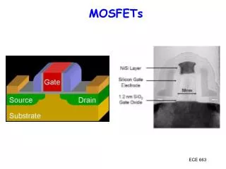
MOTIVATION The FD-SOI becomes an attractive choice for small research groups and SME’s, where research projects related to ASICs /MEMS integration arecarried out. A MOSTXX application for MOSFET parameter extraction has been developed in the ITE as a cost effective tool for characterization of the CMOS ICs. Recently the EKV model, has been implemented. The paper reports results of EKV model parameter extraction for the FD-SOI MOSFETs. The analysis has been done using the MOSTXX software.
MOSTXX application • Integration with MS Excel • „Local” extraction: • Threshold voltage • Mobility • „Global” extraction: • MOSFETs parameters • Diodes parameters (I-V, C-V) • Extraction of dimensions variations using sets of devices Area component Edge component
EKV MODEL IMPLEMENTATION The EKV model accounts for weak and strong inversion ranges and is based on interpolation of F(v) The Oguey, Cserveny approximation The approximation in the EKV enhanced in order to calculate F”(v)
TECHNOLOGY 0.75÷2 µm FD-SOI CMOS process onSmartCut UNIBOND wafers. Semi-recessed LOCOS used to isolate the devices. n+-poly-Si gate material Boron implantation of the n- and p-channel MOSFETs Basic parameters of the process: Buried oxide thickness TBOX= 400 nm Final thickness of the silicon film TSi= 80 nm Gate oxide thickness TOX= 31 nm Junction depth XJ= TSi(assumed)
DEVICES I(VGS) data of intrinsic(I-type) n- and p-channel MOSFETs I(VGS) data of highly doped (P12-type) n- and p-channel MOSFETs
DEVICES I(VDS) data of P2- and P12-type n-channel MOSFETs; cumulative boron implantation gives so high boron concentration in the Si film, that “kink-effect” appears
SUMMARY The EKV model implemented in optimization tool may be useful for characterization of FD-SOI MOS transistors. The results of extraction of FD SOI MOSFETs parameters: Square-root VT(VB) dependence should be revised P-channel MOSFETs devices will be characterized • GAM, PHI parameters estimated “manually” because of too small number of back gate bias voltages. • VTO, KP, UCRIT, LAMBDA related to boron concentration • NUO is below 1, except of I-type device
Thanks a lot for your attention Acknowledgement The authors would like to express thanks to Dr Władysław Grabiński from Geneva Modeling Center, Freescale for encouragement towards this work and helpful discussions during its preparation. http://www.ite.waw.pl dtomasz@ite.waw.pl