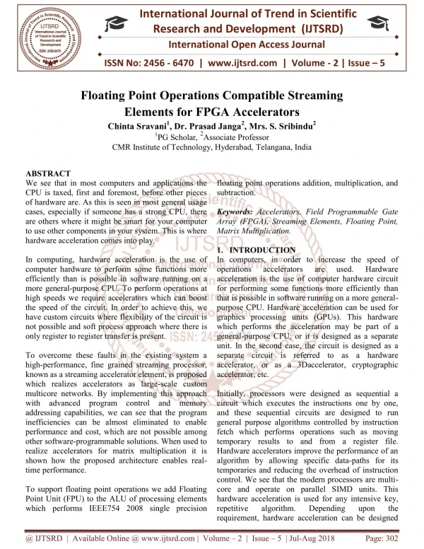
Floating Point Operations Compatible Streaming Elements for FPGA Accelerators
80 likes | 105 Vues
We see that in most computers and applications the CPU is taxed, first and foremost, before other pieces of hardware are. As this is seen in most general usage cases, especially if someone has a strong CPU, there are others where it might be smart for your computer to use other components in your system. This is where hardware acceleration comes into play. In computing, hardware acceleration is the use of computer hardware to perform some functions more efficiently than is possible in software running on a more general purpose CPU. To perform operations at high speeds we require accelerators which can boost the speed of the circuit. In order to achieve this, we have custom circuits where flexibility of the circuit is not possible and soft process approach where there is only register to register transfer is present. To overcome these faults in the existing system a high performance, fine grained streaming processor, known as a streaming accelerator element, is proposed which realizes accelerators as large scale custom multicore networks. By implementing this approach with advanced program control and memory addressing capabilities, we can see that the program inefficiencies can be almost eliminated to enable performance and cost, which are not possible among other software programmable solutions. When used to realize accelerators for matrix multiplication it is shown how the proposed architecture enables real time performance. To support floating point operations we add Floating Point Unit FPU to the ALU of processing elements which performs IEEE754 2008 single precision floating point operations addition, multiplication, and subtraction. Chinta Sravani | Dr. Prasad Janga | Mrs. S. SriBindu "Floating Point Operations Compatible Streaming Elements for FPGA Accelerators" Published in International Journal of Trend in Scientific Research and Development (ijtsrd), ISSN: 2456-6470, Volume-2 | Issue-5 , August 2018, URL: https://www.ijtsrd.com/papers/ijtsrd15853.pdf Paper URL: http://www.ijtsrd.com/engineering/electronics-and-communication-engineering/15853/floating-point-operations-compatible-streaming-elements-for-fpga-accelerators/chinta-sravani<br>

Floating Point Operations Compatible Streaming Elements for FPGA Accelerators
E N D
Presentation Transcript
International Research Research and Development (IJTSRD) International Open Access Journal Floating Point Operations Compatible Streaming Elements for FPGA Accelerators Chinta Sravani1, Dr. Prasad Janga2,Mrs. S. Sribindu2 PG Scholar,2Associate Professor CMR Institute of Technology, Hyderabad,Telangana, India International Journal of Trend in Scientific Scientific (IJTSRD) International Open Access Journal ISSN No: 2456 ISSN No: 2456 - 6470 | www.ijtsrd.com | Volume 6470 | www.ijtsrd.com | Volume - 2 | Issue – 5 Floating Point Compatible Streaming Elements f Chinta Sravani 1PG Scholar, CMR Institute of Technology, Hyderabad, ABSTRACT We see that in most computers and applications the CPU is taxed, first and foremost, before other pieces of hardware are. As this is seen in most general usage cases, especially if someone has a strong CPU, there are others where it might be smart for your to use other components in your system. This is where hardware acceleration comes into play. In computing, hardware acceleration is the use of computer hardware to perform some functions more efficiently than is possible in software running on more general-purpose CPU. To perform operations at high speeds we require accelerators which can boost the speed of the circuit. In order to achieve this, we have custom circuits where flexibility of the circuit is not possible and soft process approach only register to register transfer is present. To overcome these faults in the existing system a high-performance, fine grained streaming processor, known as a streaming accelerator element, is proposed which realizes accelerators as large- multicore networks. By implementing this approach with advanced program control and memory addressing capabilities, we can see that the program inefficiencies can be almost eliminated to enable performance and cost, which are not possible amo other software-programmable solutions. When used to realize accelerators for matrix multiplication it is shown how the proposed architecture enables real time performance. To support floating point operations we add Floating Point Unit (FPU) to the ALU of processing elements which performs IEEE754 2008 single precision floating point operations addition, multiplication, and subtraction. Keywords: Accelerators, Field Programmable Gate Array (FPGA), Streaming Elements, Floating Point, Matrix Multiplication. 1. INTRODUCTION In computers, in order to increase the speed of operations accelerators acceleration is the use of computer hardware circuit for performing some functions more efficiently than that is possible in software running on a more general purpose CPU. Hardware acceleration can be used for graphics processing units (GPUs). This hardware which performs the acceleration may be part of a general-purpose CPU, or it is designed as a separate unit. In the second case, the circuit is designed as a separate circuit is referred to as a hardware accelerator, or as a 3Daccelerator, cryptographic accelerator, etc. Initially, processors were designed as sequential a circuit which executes the instructions one by one, and these sequential circuits are designe general purpose algorithms controlled by instruction fetch which performs operations such as moving temporary results to and from a register file. Hardware accelerators improve the performance of an algorithm by allowing specific data temporaries and reducing the overhead of instruction control. We see that the modern processors are multi core and operate on parallel SIMD units. This hardware acceleration is used fo repetitive algorithm. requirement, hardware acceleration can be designed ent, hardware acceleration can be designed We see that in most computers and applications the CPU is taxed, first and foremost, before other pieces of hardware are. As this is seen in most general usage cases, especially if someone has a strong CPU, there are others where it might be smart for your computer to use other components in your system. This is where floating point operations addition, multiplication, and Accelerators, Field Programmable Gate Array (FPGA), Streaming Elements, Floating Point, In computing, hardware acceleration is the use of computer hardware to perform some functions more efficiently than is possible in software running on a purpose CPU. To perform operations at high speeds we require accelerators which can boost the speed of the circuit. In order to achieve this, we have custom circuits where flexibility of the circuit is not possible and soft process approach where there is only register to register transfer is present. In computers, in order to increase the speed of operations accelerators acceleration is the use of computer hardware circuit for performing some functions more efficiently than that is possible in software running on a more general- se CPU. Hardware acceleration can be used for graphics processing units (GPUs). This hardware which performs the acceleration may be part of a purpose CPU, or it is designed as a separate unit. In the second case, the circuit is designed as a ate circuit is referred to as a hardware accelerator, or as a 3Daccelerator, cryptographic are are used. used. Hardware Hardware To overcome these faults in the existing system a performance, fine grained streaming processor, known as a streaming accelerator element, is proposed -scale custom multicore networks. By implementing this approach with advanced program control and memory addressing capabilities, we can see that the program inefficiencies can be almost eliminated to enable performance and cost, which are not possible among programmable solutions. When used to realize accelerators for matrix multiplication it is shown how the proposed architecture enables real- Initially, processors were designed as sequential a circuit which executes the instructions one by one, and these sequential circuits are designed to run general purpose algorithms controlled by instruction fetch which performs operations such as moving temporary results to and from a register file. Hardware accelerators improve the performance of an algorithm by allowing specific data-paths for its temporaries and reducing the overhead of instruction control. We see that the modern processors are multi- core and operate on parallel SIMD units. This hardware acceleration is used for any intensive key, algorithm. To support floating point operations we add Floating U of processing elements which performs IEEE754 2008 single precision Depending Depending upon upon the the @ IJTSRD | Available Online @ www.ijtsrd.com Available Online @ www.ijtsrd.com | Volume – 2 | Issue – 5 | Jul-Aug 2018 Page: 302
International Journal of Trend in Scientific Research and Development (IJTSRD) ISSN: 2456-6470 from a small functional unit, to a large functional block. There is a tradeoff between flexibility and efficiency. The assets accessible inside present day FPGA, which might be utilized to form the accelerators, are uncommon: per-second access to trillions of multiply– gather (MAC) tasks and bit-level memory areas through on-chip DSP units and block RAM (BRAM). These check FPGA as perfect hosts to superior custom registering designs for flag, picture, and information preparing. Be that as it may, as the scale and the advancement of FPGA gadgets increment with each passing age, saddling these assets turns out to be progressively accomplishing essential execution and cost has required manual outline of custom circuits at enroll move level in an equipment plan dialect. This is an exceedingly viable approach, overwhelming improvement stack because of the low level of outline reflection. Soft processors have been proposed to lighten this plan burden by employing a predominately software- based development course, yet at introduce, embracing such an approach requests significant trade off on performance and cost. No approach has been appeared to help execution and cost even near custom circuits planned through the customary approach. To resolve this issue a novel streaming accelerating element (SAE) is introduced which empowers programming based streaming element advancement, while keeping up the execution and cost of custom circuits. By application of streaming elements for matrix multiplication (MM), the accompanying commitments are made. 1.A novel streaming processor for FPGA, the SAE, is depicted and appeared to conquer the execution confinements of existing soft processors. 2.It is indicated how the SAE is exceptional among soft cores in empowering ongoing accelerators, for example, H.264 video. 3.It is indicated how SAE-based accelerators are one of a kind in showing execution and cost which are profoundly focused with custom circuits. 4.It is demonstrated how SAE show execution and cost up to two requests of extent past that of existing delicate processors. To the best of our insight, the SAE is the most noteworthy execution, least cost programming programmable segment on record for FPGA and the first to empower signal and image handling streaming elements with execution and cost comparable with custom circuits. 2. Background: Among the accelerators, the one which is most performance based is custom circuits. Custom circuit accelerators are those which have a hardware designed for a specific function. As it is designed for a specified application, flexibility of this processor is nonexistent and cost of manufacturing for these types of circuits is more. In order to have flexibility and to reduce the cost of manufacturing we have approached a procedure which is software based softcore processors. These softcore processors do not show the good performance efficiency. Hence, we consider incorporating the processing elements which can cooperate for SISD and SIMD operations for a proper defined flow to improve the efficiency. The FPGA processing elements are designed which show a path for data flow but even these approaches have delays which effect the performance efficiency. For avoiding such problems and to implement a circuit which can give its performance efficiency which can be equal to that of custom circuits we go for streaming accelerator elements approach. Let us see the approach from where the idea has been implemented and its effects which result in implementing a circuit with streaming accelerating elements In any case, acknowledging high performance in accelerators has generally required manual custom circuit register to register transfer level procedure which made progressively ineffective by the size of present day FPGA. For instance, high level synthesis (HLS) approaches improve this procedure by getting accelerators from specifications in, for example, C/C++, CUDA, OpenCL, or Java. The efficiency benefits of HLS are unchallenged, however there is no convincing proof that these can bolster execution and cost practically identical with custom circuits, while the necessity for a host processor for any CUDA or OpenCL program forces high asset and execution overheads. An alternative approach is to acknowledge software programmable processors in the FPGA programmable logic. These softcore processors enable their engineering to be tuned before union to enhance the execution and cost of the final result. Their utilization is attractive in occasions where HLS approaches are compelled—for example when specific automatic develops, for example, pointers, are utilized which can't be blended by HLS approaches. Likewise, softcore processors have been difficult. Customarily, yet forces an @ IJTSRD | Available Online @ www.ijtsrd.com | Volume – 2 | Issue – 5 | Jul-Aug 2018 Page: 303
International Journal of Trend in Scientific Research and Development (IJTSRD) ISSN: 2456-6470 appeared to empower performance scaling beyond that of HLS . It creates the impression that if FPGA softcore processors are to be a reasonable other option to custom accelerators, at that point execution and cost must enhance profoundly. The first advance toward that path, is sharing a few qualities of these non- FPGA-based structures, specifically the utilization of huge scale multicore systems and task on floods of information. It endeavors to reconsider these for the acknowledgment of custom FPGA accelerators. It utilizes alleged processing elements (PEs) amazingly fine-grained processors joining these into substantial scale impromptu multi-PE architectures. A PE is not a general-purpose softcore processor, however is intended to empower programming programmability with most reduced asset cost, while amplifying execution and scaling. This approach is promising, it is the main processor based real time solution, and execution and cost were profoundly focused with similar custom circuits for any application, but still a general capacity to empower execution and cost equivalent with custom circuits isn't in prove. This paper proposes a way to deal with settle this issue. 3. FPGA PROCESSING ACCELERATORS same or unique PEs, while the multicore point-to- point topology is customized before amalgamation proper to the activity being figured it out. Acknowledging structures of this kind efficiently requests two key PE highlights. 1.Standalone: A PE must have the capacity to process information, oversee memory access, and impart remotely under programming control without a host processor. 2.Lean: Combined high efficiency with low cost are requested to help vast scale multicores. None of the softcore processors fulfill both of these criteria. One such which does is the FPGA PE (FPE). 3.2. The FPGA Processing Element: The FPE instruction set architecture is a RISC load store PE, SIMD, and SISD (i.e., single-path SIMD) variations of which are shown in Fig. 3.2. This architecture composes of program counter (PC), program memory (PM), Instruction decoder (ID), branch detection, Data Memory (DM), immediate memory, and an ALU in view of the DSP48E in Xilinx FPGA. A COMM (communication) module inclusion/extraction of information into and out of the FPE pipeline. The FPE is extremely lean, fusing just those parts basic to programming programmability. Register File (RF), allows coordinate ELEMENT Fig 3.1 Multicore PE accelerator architecture 3.1 FPE Accelerators: The above figure demonstrates the reasonable multi- PE accelerator design is proposed. As this shows, these are made out of numerous PEs conveying by means of a point-to-point organize made out of first- input, first-output (FIFO) lines. A PE (Processing Element) is a software programmable single instruction multiple data (SIMD) part whose design is delicate for configuration pre synthesis in various perspectives, most remarkably number of SIMD paths. Every PE embraces autonomous of all others and PE execution is decoupled, to such an extent that the system is a heterogeneous various direction, multiple data (MIMD) machine. Point-to-point joins are made between conveying paths whether housed inside the Fig 3.2 FPE in SISD mode a configuration Fig 3.3 FPE in SIMD mode By guaranteeing total most minimal cost FPE structure, the economies of scale deliver sensational @ IJTSRD | Available Online @ www.ijtsrd.com | Volume – 2 | Issue – 5 | Jul-Aug 2018 Page: 304
International Journal of Trend in Scientific Research and Development (IJTSRD) ISSN: 2456-6470 diminishments in multicore asset cost. Be that as it may, this outrageous concentration comes at the cost of flexibility: once blended, the FPE does not show an indistinguishable level of flexibility from a general delicate processor in light of the fact that the engineering is exceptionally configuration time to help the coveted task with most astounding execution and least cost; henceforth, while it might be reprogrammed after blend, it can't empower broadly useful activity in the way of a standard softcore. Likewise, to limit cost while supporting programming programmability, the FPE works under two considerable outright confinements. 1.Processor and ISA: The FPE is a load store processor which can just source non-consistent ALU operands and deliver results to RF. 2.Addressing Modes: The FPE underpins just direct memory addressing. 3.3 Instruction set Architecture: Instruction Set Architecture (ISA) is a theoretical model of a PC. It is likewise alluded to as design or PC engineering. An acknowledgment of an ISA is called a usage. An ISA licenses different execution that may change in execution, physical size, and cost (in addition to other things); in light of the fact that the ISA fills in as the interface amongst programming and equipment. Programming that has been composed for an ISA can keep running on various executions of the same ISA. These advancements have brought down the cost of PCs and to build their appropriateness. Thus, the ISA is a standout amongst the most imperative deliberations in processing today. An ISA characterizes everything a machine dialect developer has to know so as to program a PC. What an ISA characterizes contrasts between ISAs; when all is said in done, ISAs characterize the upheld information writes, what state there is, (for example, the principle memory and registers) and their semantics, (for example, the memory consistency and tending to modes), the guideline set (the arrangement of machine directions that includes a PC's machine dialect), and the input/output demonstrate. In order to analyze the flow of the data from one block to another we need a set of instructions which can help us declare the data accordingly. compelled at Table 3.1 FPE Instruction Set 3.4 Stream Processing for FPGA Accelerators: Fig.3.4. FPE Load-store ways For complex data execution, the volume of information requires BRAM DM, all together for these operands to be handled and comes about put away, an expansive number of stores are required amongst BRAM and RF. Given the straight forwardness of the FFT butterfly activity, the extent of the program involved by these guidelines is significant. In any case, with regards to the FPE, the circumstance compounds still: since the FPE is independent and handles its own correspondence, additionally cycles are approaching and active information amongst DM and COMM, lessening program efficiency even more. At last, every one of these exchanges initiates an activity amongst source and goal—as appeared in Fig. 3.4, each FPE DM-RF (dark) and COMM-RF (red) exchange takes eight cycles, forcing the requirement for NOP guidelines. At last, these elements consolidate as far as possible the efficiency of the FPE. This situation is not unique to the FPE. In order to beat this inefficiency, two properties ought to be upheld. A.Direct access to any blend of RF, DM, and COMM for either guideline source or goal. expended exchanging @ IJTSRD | Available Online @ www.ijtsrd.com | Volume – 2 | Issue – 5 | Jul-Aug 2018 Page: 305
International Journal of Trend in Scientific Research and Development (IJTSRD) ISSN: 2456-6470 B.In situations where neighbourhood buffering isn't required, information through the PE ought to be empowered. The outline challenge is to empower these highlights without trading off on the asset efficiency required to uphold custom hardware. 4.1 Stream Accelerator Elements: To help achieve the required demands, a novel SAE is proposed. The SAE keeps up independent conduct and a product programmable lean design, however, the requirement is the capacity to stream information into and out of task sources and goals and through the ALU without the requirement for load and store cycles. This gushing takes two structures. 1.Internal: Peer/direct access to RF, DM, COMM, and IMM without the requirement for delay cycles i.e., load store cycles. 2.External: Unbuffered gushing of information from input FIFOs to output FIFOs by means of just ALU. On the off chance that these were not in a similar pipeline arrange, guideline unravel and pipeline administration would be significantly muddled to adjust the information touching base at the ALU with variable idleness. Subsequently, information operands and results might be sourced/created to any of IMM, RF, DM, or COMM with indistinguishable pipeline control and without the requirement for express load and store cycles or guidelines for DM or COMM. Fig. 4.2 SAE ALU access path Fig. 4.3 ALU with FPU Internal Block Diagram Fig. 4.1 SISD SAE Architecture In addition, in order to enable unbuffered streaming operation from input to output FIFOs through ALU, synchronous read/write with outer FIFOs is required, with access to ALU in the two bearings. Keeping in mind the end goal to help this capacity, decoupled COMMGET and COMMPUT segments are conveyed in the SAE inside FlexData. Note that these both live in a similar pipeline arrange and, consequently, fit in with the consistent dataflow pipeline kept up over the rest of FlexData. Also, since all of COMMGET, COMMPUT, DM, RF, and IMM get to unmistakable memory assets (with isolated memory banks utilized inside the SAE and a FIFO utilized per off-SAE correspondence channel), there is no memory transfer speed coming about because of decoupling. 4.2 Instruction Coding: There are multiple instructions which we are going to define which are using. As we see in the above figure there are different blocks for defining a path. By using the streaming accelerator elements in SISD approach we see that it possess three distinguish characteristics A.Independent ID block is designed.(Defined block) B.Flex Data realisation. C.Comm_get and Comm_put blocks which define a ditinguished path. In the SAE, ID and FlexData rule full pipeline stages. The ID decides the source/goal of any direction operand/result, with the greater part of the potential sources or goals of information joined in FlexData to enable each to be tended to with break even with inactivity; this flat memory engineering is interesting to the SAE and particular from that utilized by some other softcore processor. Its impact is to lessen the multifaceted nature of getting to every one of the unmistakable operand sources by means of a normal dataflow. @ IJTSRD | Available Online @ www.ijtsrd.com | Volume – 2 | Issue – 5 | Jul-Aug 2018 Page: 306
International Journal of Trend in Scientific Research and Development (IJTSRD) ISSN: 2456-6470 Control instructions – LOOP, RPT, BEQ, BGT, BLT, JMP, GET, PUT, GETCH, CLRCH, NOP. ALU instructions – MUL, ADD, SUB, MULADD, MULSUB, COPROC. MEM Instructions – LD, ST, LDIMM, STIMM, LDIAR. To permit include (yield) of information from (to) the suitable source (goal), both the physical source segment (RF, COMMGET, COMMPUT, DM, and IMM) and the fitting locations inside each (i.e., memory area or correspondence channel) must be transferred inside the guideline. To oblige this, SAE ALU directions are accompanying arrangement: INSTR dest, opA, opB where INSTR is the guideline class, dest identifies the outcome goal/output, and opA and opB recognize the source operands. 4.3.1 Program Counter A program counter is also called as instruction pointer. A program counter is an enroll in a PC processor that contains the address (area) of the guideline or instruction being executed at the present time. As every instruction or guideline gets got, the program counter builds its put away an incentive by 1. At the point when the PC restarts or is reset, the program counter typically returns to 0. In registering, a program is a particular arrangement of requested activities for a PC to perform. A direction is a request given to a PC processor by a program. Inside a PC, an address is a particular area in memory or capacity. An enlist is one of a little arrangement of information holding places that the processor employments. After fetching an instruction PC is incremented and it with holds the memory of instruction that is to be executed next. you see when the PC boots, and (frequently, yet not generally) the configuration pages where you characterize on the off chance that you have a floppy introduced, if the PC should bolster a USB console and so on. 4.3.3 Data Memory Here is where you put your factors. You can read and compose esteems. Program is guideline what CPU executes, information will be data that program utilizes for customization and capacity of how the program should convey those directions. communicated in the Fig. 4.5 Flow of PCM The structure of the SAE PC and PCM and the conduct of the PCM are appeared in Fig. 4.5. The PCM controls the refresh of the PC given its past esteem and the guideline referenced in PM given snippets of data—the begin and end lines of the body articulations to be rehashed S and E, the quantity of reiterations N. These are encoded in a RPT direction added to the SAE guideline set. These guidelines are encoded as RPT N S E. The PCM mediates the PC to guarantee the right number of redundancies of the body proclamation and to help the development of settled rehash activities by establishing the flowchart in Fig. 10. Specifically, for a n-level home, it keeps up n + 1-component arrangements of measurements, with an extra component added to help infinite reiteration of the best level program, thought to be a verifiable infinite rehash guideline. For layer I of the circle settle, the Fig.4.4. Internal PC logic 4.3.2 Program Memory Your PC likewise has data memory and program memory. However, the program memory is little in the PC - it is only for capacity of the boot messages @ IJTSRD | Available Online @ www.ijtsrd.com | Volume – 2 | Issue – 5 | Jul-Aug 2018 Page: 307
International Journal of Trend in Scientific Research and Development (IJTSRD) ISSN: 2456-6470 begin line, end line, and number of redundancies are put away in component I +1 of the rundowns s, e, and n, individually. In all cases s0 = 0, e0 =∞and n0 =∞to speak to the begin line, end line, and number of reiterations of the best level program [ in Fig. 4.5 ]. Every time a rehash guideline is experienced I, the present record into s, e, andn is increased and the estimations of the new component introduced utilizing S, E, andN from the decoded direction in (3). General PC refreshing at that point continues (1) until the point when either another rehash guideline is identified or until the point when ei is experienced. In the last case, the quantity of cycles of the present explanation is decremented (2), or if ni = 0, the majority of the emphasess of the present repeat proclamation have been finished and control of the circle settle returns to the past level (4). The pcm_en dictates whether the PCM is incorporated into the blended design or else it takes a Boolean esteem. For the situation where a PCM is incorporated, the greatest profundity of circle settle is configurable by means of pcm_en which can take, theoretically, any esteem. In that capacity, the PCM perhaps included or excluded and hence, imposes no cost when it isn't required; besides, when it is incorporated, its cost can be tuned to the current application by changing the most extreme profundity of circle settle. The signals COMMGET and COMMPUT can work tending to modes as determined via the mode parameter. In coordinate mode, singular FIFO channels by means of locations encoded inside the direction. Guidelines for either COMM unit are encoded as a) COMM_GET DEST b) COMM_PUT SOURCE Fig 4.6 Flow of channel pointer 4.4 Single Precision Representation Single precision, also called as "float" in the C language family, is a binary format that occupies 32 bits (4 bytes) and its significant has a precision of 24 bits (about 7 decimal digits). The single precision floating point format has an 8 bit exponent and 26 bit mantissa plus a sign bit. It is a 32 bit representation and its bias value is equal to 127. Figure 4.7 IEEE-754 Single Precision Floating Point Format Figure 4.8 Flowcharts for Multiplication 5. Conclusion Soft processors for FPGA experience the effects of generous degradation in performance and cost with respect to custom circuits. The SAE implemented uses a technique which allows for maximum efficiency which is compatible with the custom circuits. We are implementing this for floating point numbers which perform arithmetic operations subtraction, and multiplication multiplication. These empower efficiency routinely more than 90% and execution and cost which are practically identical with custom circuit accelerators and well ahead of time of existing soft processors. Also, it is indicated how SAE-based MM (Matrix like addition, matrix for Fig 4.6 Flow of COMMGET and COMMPUT @ IJTSRD | Available Online @ www.ijtsrd.com | Volume – 2 | Issue – 5 | Jul-Aug 2018 Page: 308
International Journal of Trend in Scientific Research and Development (IJTSRD) ISSN: 2456-6470 Multiplication) asset/cost by up to three degrees of magnitude. To the best of our insight, these capacities are extraordinary, for FPGA, as well as for any semiconductor innovation. Advantages: Delay is reduced in processing the instructions. It is more performance efficient compared to softcore processors and achieves almost as good performance as that of custom circuits. Future scope: As future work, however furthermore the FPGA accelerators might be utilized to additionally facilitate the outline procedure. For instance, programmability of the SAE implies that it might likewise be utilized as a memory controller to execute custom memory access. References 1.C. H. Chou, A. Severance, A. D. Brant, Z. Liu, S. Sant, and G. G. F. Lemieux, "VEGAS: Soft vector processor with scratchpad memory," in Proc. nineteenth ACM/SIGDA Program. Entryway Arrays (FPGA),2011 accelerators offer changes in Reconfigurable Technol. Syst., vol. 7, no. 3, Aug. 2014, Art. ID 19 4.P. Wang and J. McAllister, "Delicate center stream processor applications," in Proc. IEEE Workshop Signal Process. Syst. (Tastes), Oct. 2013 for sliding window 5.X. Chu and J. McAllister, "Programming defined circle unraveling for location," IEEE Trans. Flag Process., vol. 60, no. 11, Nov. 2012. FPGA-based MIMO Author Profile: Chinta Bachelor’s Degree in 2015 from Electronics and Communication of Engineering from Aeronautical Engineering. She is pursuing M. Tech in VLSI System Design from CMR Institute of Technology Sravani. She received Institute of Dr. Prasad Janga. He received Bachelor’s from V.R. Siddhartha Engineering College accomplished Master’s Degree from SITAMS. He is pursuing PhD from (NIU)-Delhi. He has an academic experience of 9 years in teaching field and is working as Associate Professor in CMR Institute of Technology. Mrs. S. SriBindu. She is working as an Associate Professor in CMR Institute Int. Symp. Field and has 2.A. Severance and G. Lemieux, "VENICE: A reduced vector processor for FPGA applications," in Proc. Int. Conf. Field-Program. Technol. (FPT), Dec. 2012 3.H. Y. Cheah, F. Brosser, S. A. Fahmy, and D. L. Maskell, "The iDEA DSP square based delicate processor for FPGAs," ACM Trans. of Technology. @ IJTSRD | Available Online @ www.ijtsrd.com | Volume – 2 | Issue – 5 | Jul-Aug 2018 Page: 309