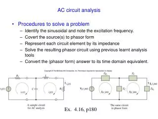
AC circuit analysis
AC circuit analysis. Procedures to solve a problem Identify the sinusoidal and note the excitation frequency. Covert the source(s) to phasor form Represent each circuit element by its impedance Solve the resulting phasor circuit using previous learnt analysis tools

AC circuit analysis
E N D
Presentation Transcript
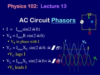
AC circuit analysis • Procedures to solve a problem • Identify the sinusoidal and note the excitation frequency. • Covert the source(s) to phasor form • Represent each circuit element by its impedance • Solve the resulting phasor circuit using previous learnt analysis tools • Convert the (phasor form) answer to its time domain equivalent. Ex. 4.16, p180
Example a. Calculate the current through the capacitor and inductor. b). If 10V and 5V batteries are replace by V1=10Vcos(1000t) and V2=5Vcos(1000t), respectively, calculate the current through the capacitor.
i v(t) e e/R 0.63e 0.63 e/R t t t=RC=t t=RC=t Charging a Capacitor Time constant (t): time needs to charge a capacitor to 63% of its full charge. The larger the RC, the longer it takes to charge a capacitor. The larger the R value, the smaller the current is in the circuit. The larger the C value, the more the charge the capacitor can hold
i=0 i ++++ ++++ Vc=e Vc=e e e vC(t) ---- ---- t = 0 e t Discharging a Capacitor
Example a) A young MacGyver enthusiast is attempting to design a simple switched RC circuit to use as a fuse timer. The child has a 5 F capacitor and one AAA cell with an emf of 1.5 V and an internal resistance of 0.6 ohm. If the fuse will ignite when the capacitor is charged to a voltage of 1.0 V, how much time does the youngster have to vacate the premises? b). With a never ending enthusiasm for adding batteries to a circuit, the youngster connects a fresh 9 V lithium battery as shown. Now how much time expires after switch closure until the fuse is ignited?
Example a) A young MacGyver enthusiast is attempting to design a simple switched RC circuit to use as a fuse timer. The child has a 5 F capacitor and one AAA cell with an emf of 1.5 V and an internal resistance of 0.6 ohm. If the fuse will ignite when the capacitor is charged to a voltage of 1.0 V, how much time does the youngster have to vacate the premises? b). With a never ending enthusiasm for adding batteries to a circuit, the youngster connects a fresh 9 V lithium battery as shown. Now how much time expires after switch closure until the fuse is ignited?
AC Power Average power rms value • The average ac power (Pav) is the power dissipated on the load resistor. • 0cosq1, dependent on the complex load. • ideal power factor: cosq =1, Z=R, pure resistive load
Review cont.: Complex Power Instantaneous power p(t) Pay attention to complex conjugate • real power Pav: power absorbed by the load resistance. • Q (volt-amperes reactive, VAR): exchange of energy between the source and the reactive part of the load. No net power is gained or lost during the process. • S : compute by measuring the rms load voltage and currents without regard for the phase angle. • if Q<0, the load is capacitive, Q>0, the load is inductive
Topic 2: Digital Circuit: Combinational Logic • Logic operation • Real problem to truth table • Karnaugh Map: • Box “1” or box “0” • Largest supercell possible • 2n ones or zeros in each supercell • Edges of Karnaugh map are connected • Finish all ones or zeros • Doesn’t matter (“d” or “x”) can be considered as either “1” or “0”.
Digital Circuit Review: Sequential Logic • Flip Flips • Timing diagram • When CLK signal arrives (rising edge or falling edge), FF will have outputs (Q and Q’) depending on the input (ex. D, or J, K). At this stage, ignore combinational logic if there exist in the circuit. • After finishing the output (Q and Q’), then work on the combinational logic, which typically determines the inputs (ex. D, or J, K) which will determine the output (Q and Q’) at next CLK signal • Sequential circuit design: State Map • Construct a state map. • Convert the state map to truth map. Note: have to include all combination. Ex. If there are three outputs, Q0, Q1, and Q2, then there are 8 states (combinations) that have to be listed. Some of them may be listed as “d”. • Prepare the inputs such that the outputs (Q0, Q1, and Q2) at next state will follow the state map. • Convert the truth map to Karnaugh map: the inputs of FF (ex, D, or J, K) is the results in Karnuagh map, i.e. the value of the inputs of FF goes into cells. The outputs of FF is the inputs in the Karnaugh map.
Example: Combinational Logic • Problem 2 of Exam 2: