Modulator-Based, High Bandwidth Optical Links for HEP Experiments
340 likes | 524 Vues
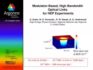
Modulator-Based, High Bandwidth Optical Links for HEP Experiments G. Drake, W. S. Fernando , R. W. Stanek ,D. G. Underwood High Energy Physics Division, Argonne National Lab, Argonne, Il, United States. Log(BER). Noise (mV). Nice open eye at BER=10 -18. Jitter (ps).

Modulator-Based, High Bandwidth Optical Links for HEP Experiments
E N D
Presentation Transcript
Modulator-Based, High Bandwidth Optical Links for HEP Experiments G. Drake, W. S. Fernando , R. W. Stanek ,D. G. Underwood High Energy Physics Division, Argonne National Lab, Argonne, Il, United States Log(BER) Noise (mV) Nice open eye at BER=10-18 Jitter (ps) For a link at 10 Gb/s - - 10-18 BER =1 error in ~1000 days ! 10-12 BER = ~ 900 errors per day !
Electro-Optical Modulators • Two methods for optical data transmission • Direct modulation of light: common in short distance, short wave length communication, all current LHC experiments use this technology • Indirect modulation of light: long distance, long wave length communication. ATLAS TileCal will test this technology in 2013 (demonstrator) for use in Phase 2 upgrade Current driver Laser (VCSEL) Optical Tx Elec. Tx Receiver PIN diodes Optical Rx Elec. Rx Laser (CW) Elec. Tx Modulator Voltage driver Optical Tx Elec. Rx PIN diodes Receiver Optical Rx Monolithically integrated Silicon photonic device 2
Two main types of Modulators • Mach–Zehnder interferometer based ΔVoltage Δrefractive index phase amplitude Pockels effect, Kerr effect, free carrier dispersion effect Materials: LiNbO3, Si, InP • Absorption based ΔVoltage Δoptical absorption Franz-Keldysh (FK) effect in bulk semiconductors and quantum-confined Stark effect (QCSE) in quantum-well (QW) structures. Materials: InP, SiGe, Graphene Output Input 3
Modulating Materials for HEP • LiNbO3 - based on the crystal property • High bandwidth, tested rad-hard, very long (~5 cm), expensive, high drive voltages • InP - based on the crystal property • Very High bandwidths, should be rad-hard, small (~2 mm), low drive voltages, expensive at present, special-purpose technology • Si - based on the free carrier dispersion effect • High bandwidth, rad-hard (?), small (~1 mm), inexpensive, could monolithically integrate, commercially available, use existing Si Technology 4
Reliability • Modulators are very simple and reliable. No known failure mechanisms • e.g. Luxtera transceiver MTBF > 2.3 x 10⁹ hrs (300 million device hours accumulated without a single intrinsic failure) • E.g. 1 device failure in TileCal >34 years (9 months running, 1024 transceivers) VCSEL Photonic Si modulator 5
Other Considerations • SM fiber is more rad-hard and cheaper than most MM fiber. Ge doped MM fiber is $ • Lasers designed to run as CW can be more reliable than switched VCSELs. Also eliminates chirp. • CW lasers can be at the Modulator or remote, depending on Radiation level.
Modulator Selection for ATLAS TileCal We propose to implement optical links to be used in the TileCal Phase 2 upgrade based on Luxtera’s silicon photonic transceiver. This comes in a standard QSFP package which can be easily plugged into a motherboard. We are doing a Demonstrator. 9.8 mm 4 x 10Gb/s transceiver from Luxtera, 130nm Silicon on Insulator (SOI) 7 • Modulator selection based on several criteria: • Availability: COTS devices 1st choice • Reliability: Proven in the field • Radiation tolerance: ~100 krad TID, ~1012 p/cm2(and rad-hard SM fibers are cheaper than doped MM) • Cost: Cost Savings over SNAP12 Baseline • Implementation: Ease over Baseline • Bandwidth: 56 Gb/s per readout board • BER: minimal correction needed 7
Commercial Integrated Optics Chips are a Promising Form of Modulators. Speed 10 + Gb/fiber commercial integrated optics 40 Gb/fiber with other commercial units Laser reliability Either CW laser onboard Or displace laser outside detector. (DFL has Different junction structure than VCSELs) Low Bit Error Rate 10-18 vs typical 10-12 for current systems Simplified error correction schemes Low power One CW laser - split many ways Modulators are very efficient Short electrical paths – no cable drivers Low voltage drivers – not current Rad hard optical parts We have tested silicon integrated optics for >64 krad application Modulator parts should work at much higher levels Optical part expected to work at multi-Mrad • 4 transmit and 4 receive fibers on one integrated optics silicon chip • 10Gb/s each fiber • Use of modulators and CW laser • Low power, small size 1 cm 1 cm laser
ANL Bench Tests of Quality and BER of the Complete Link(Modulator & Receiver with 200m SM fiber) FPGA board generate PRBS7 bit stream @10.3125 Gb/s QSFP Interface board Tx 4 SMA cables to Tx Luxtera Mod 4 SMA cables from Rx Rx Use FPGA to generate random bit stream 4 input ports, 4 output ports. SMA 8 SM fiber bundle DSA8200 Communication Analyzer 100 m Scope to monitor Quality (eye diagram) and calculate Bit Error Rate (BER) Feedback 9
Eye diagram of Complete Link Mask 140% of 10GBASE-R The quality of the link is measured and compared with IEEE 802.3ae and the performance exceeds the requirements by 40% more 10
Verified* Luxtera 10-18 BER Spec 10-18 BER =1 error in ~1000 days ! 10-12 BER = ~ 900 errors per day Per link @ 10 Gb/s ANL test Luxtera / Molex Test Log(BER) • Why is Low BER important ? • High BER requires Forward Error Correction (FEC) which consumes 30% of the bandwidth and requires error correction which consumes power and introduce susceptibility to radiation • BER < 10-18 ~ ~ no need for FEC -> save money and bandwidth and more rad-hard! Noise (mV) Nice open eye at BER=10-18 Jitter (ps) • Achieved: • Per Link 10Gb/s (faster by x2 the upgrade target) • BER < 10-18 (better by x106 over upgrade performance) • Lower power consumption (factor of x6 the upgrade target) 11
Summary of Comparison Per fiber * Estimate 12
Overall Plan for Demo of Luxtera / Molex QSFP Modulator based Devices On-Detector Counting House 200 M
A Proposed Interface to the TileCal Main Board 6 Note Extra I2C and monitor links through QSFP connector to emulate non-rad-hard PIC uC TO USA15 Luxtera QSFP connector Stockholm and Valencia are now designing the mainboard and ROD to accommodate the Luxtera QSFP package. ADC low gain ADC hi gain 6 differential serial links (4 Tx, 2 Rx) shaper Integrator charge injection PMT FPGA (Kintex-7) Serializer & Control 12 tubes 12 bit ADCs Includes duplicate backup links ADC low gain ADC hi gain shaper Integrator charge injection PMT Integrator multiplexer Integrator ADC Luxtera QSFP has 4 x 14 Gb/s transceivers QSFP: Quad Small Form Factor Pluggable Inside ATLAS Tilecal Iron Girder 14
First Steps of ANL Radiation Test Program Links run continuously at 10 Gb/s during irradiation 3 technologies Integrated Silicon – CMOS (4-channel) InP single channel LiNO3 single channel Proton Beam Electron Beam NO SEE @ 1012 protons/cm2 & 64 krad TID OK after ~100 krad TID and 3.5 x min ionizing
Levels of Radiation Sensitivity in Modulator-based COTS devices • Modulator • Logic and RF circuitry in Modulator chip • Attached CW Laser • Voltage regulators • Glue, Capacitors, etc • Control Unit ( PIC uC or..) • Working Group Wednesday 16:00 Only issue so far
In this Luxtera / Molex device uC is used for startup reads and sets parameters for operation also allows readout of temperature, current, etc After startup, the device will continue to operate until power down (or perhaps some large change in device) We can use external I2C, etc through spare pins on QSFP connector to eliminate uC
USB Shielded from radiation ~100 m CW Lasers 8 SMA 8 SMA USB 12 V I2C 2 x Differential I2C PM Fiber QSFP QSFP SMA 8 Fiber Fiber SM LiNbO3 Fiber SM InP 2 Fibers SM QSFP Radiation Exposure Region Electrical feedback Monitoring optical power, Voltages, currents 4 x 10Gb/s BER testing PC FPGA board QSFP board I2C Main + Power I2C QSFP connect Receivers
Summary: Modulators • Modulators are a robust replacement for VCSEL-based optical readout: • High Speed: >10 Gb/s. No speed limits • Reliable: Rad hard, BER ~10-18. MTBF ~2.3 x 10⁹ hrs • We have proposed an optical link be used in TileCal and have built a prototype link based on Luxtera transceiver • Characterized it for use @ 10 Gb/s with < 10-18 BER • Tested radiation hardness up to 8 x 10¹¹ p/cm2 • No SEU at this level • Need some changes to the controller ---- • Investigating other COTS modulator devices made of other materials. • Investigating options to use modulators in very high radiation environments such as tracker upgrades 19
Development of Free-Space (fiberless) Links Utilizing Modulators • Advantages: • Low latency (no velocity factor) • Work over distances from few mm (internal triggers) to ~Km (counting house) or far ( to satellite orbit) • Low mass • No fiber routing • Communicate between ID layers for trigger decisions. 20
A trigger concept using modulators and prisms Data path for on-board tracking trigger which could couple 2 planes of 3D doublets.
MEMS Mirrors for steering over ~ order 1 M distance A commercially available MEMS mirror (Developed at ARI, Berkeley) Argonne Center for Nan-scale Materials (CNM) developed novel MEMS mirrors that should solve the problems of commercial mirrors. The mirror is supported laterally and it can be actuated using 4 torsional actuators. October 6, 2014 22 22
A nice demonstration 1 Gb/s to a target moving ~1 cm at > 100 Hz Reflective lens Reflection 850 nm LASER For alignment This Assembly moves X optical electric ADC TIA SFP Rigid Coupling Y Si Detectors SPI Small Prism GRIN lens to Capture wires FPGA Bit Error Tester FPGA 1550 LASER Beam Lookup table Digital filter SPI wires X Asphere Lens to launch MEMS Mirror to steer DAC Amp Y Modulator No Bit errors overnight CW LASER 1550 nm 23 23
ANL Long Range Free-Space Communication Telescope Demo 1 Gb/s over 80 Meters 24 24
Modulator Plans • Radiation Test Luxtera Molex without the microcontroller Protons 3.5 x min ioni. Gammas total dose up to 3 MR Neutrons • Radiation test components of Luxtera/Molex Voltage Regulator Laser ATLAS Tilecal Demonstrator Tests Kintex 7 FPGA Radiation test Other Devices and other materials For higher radiation environments Develop other Optical Communication capabilities
Summary Modulators are simple, reliable, fast Silicon Integrated Technology exists for some HEP applications For ATLAS Tilecal demonstrator we expect: factor 106 lower BER, factor ~ 3 cost savings factor ~ 6 power savings simplification We are continuing to test commercial and other modulators Have demonstrated precise beam steering with MEMS mirrors 26
References [1] KK. Gan, F. Vasay, T Weidberg, “Lessons Learned and to be Learned from LHC”, Joint ATLAS-CMS Working Group on Opto-Electronics for SLHC, ATL-COM-ELEC-2007-001 CMS-IN-2007/066 [2] Philippe Farthouat’s 2011 ATLAS upgrade talk [3] T. Weidberg “VCSEL Reliability Studies and Development of Robust VCSEL Arrays” TWIPP 2011 [4] W. Fernando, “Overview and status of ATLAS pixel detector”, Nucl.Instrum.Meth., A596, 58-62 (2008) [5] D. Giugni, S. Michal, R. Boyd, ATLAS PIXEL nSQP Project, ATL-IP-ES-0150 [6] Papotti et. al ,“An Error-Correcting Line Code for a HEP Rad-Hard Multi-GigaBit Optical Link”, 12th Workshop on Electronics For LHC and Future Experiments, Valencia, Spain, 25 - 29, pp.258-262 (2006) [7] Molex specifications (http://www.molex.com/molex/products/family?key=fourteen_data_rate_fdr__active_optical_cable_aoc&channel=products&chanName=family&pageTitle=Introduction&parentKey=fiber_optic_product_families) [8] J. Gilmore, TMB Mezzanine SEU Testing - Preliminary Results (www.physics.ohio-state.edu%2F~gilmore%2Fcms%2Fregulators%2Fcyclotron_report_v2.ppt) [9] W. Pascher et al., “Modelling and design of a travelling-wave electro-optic modulator on InP”, Opt. Quant. Electron., vol. 35(4), 453-464 (2003) [10] R. A. Soref and B.R. Bennett , “Electrooptical Effects In Silicon”, J. Quantum Electron., 23, 123 (1987) [11] M. Bruzzi, "Radiation damage in silicon detectors for high-energy physics experiments," Nuclear Science, IEEE Transactions on , vol.48, no.4, pp.960-971, Aug 2001 [12] S.T. Liu et al., "Total dose radiation hard 0.35 μm SOI CMOS technology," Nuclear Science, IEEE Transactions on , 45(6), 2442-2449 (1998) [13] F Vasey et al, “The Versatile Link common project: feasibility report”, JINST 7 C01075 (2012) doi:10.1088/1748-0221/7/01/C01075 [14] HHI specifications (http://www.hhi.fraunhofer.de/en/departments/photonic-components/inp-modulators/) [15] T. Pinguet et al. , "Monolithically integrated high-speed CMOS photonic transceivers," Group IV Photonics, 2008 5th IEEE International Conference on , vol., no., pp.362-364, 17-19 Sept. 2008 [16] C. Gunn, et al., “A 40Gbps CMOS Photonics Transceiver”, Proceedings of SPIE 6477, 64770N (2007). [17] BT Huffman et al.The Radiation Hardness of Certain Optical Fibres for the LHC Upgrades at -25C. JINST 2010 5 C11023. 28
References RD23 Collaboration, “Optoelectronic Analog Signal Transfer for LHC Detectors”. CERN/DRDC/91-41/DRDC/P31. CERN, Geneva 1991. [PIXEL]W. Fernando, “Overview and status of ATLAS pixel detector”,. Nucl. Instrum.Meth 2008; 58-62: A596. [KK] K.K.Gan, W. Fernando, H. Kagan, R. Kass, A. Law et al, “Radiation-Hard Optical Link for SLHC”. Nucl.Instrum.Meth,2008:88, 2008:88-92:A596. L.S. Yan, Q.Yu, A.E.Willner (UCLA), "Simple Measurement of the Chirp Parameter of Optical Modulators Using Partial Optical Filtering", Optoelectronics and semiconductor integrated Devices, P2.28, IEEE. [CHIRP] "Simple Measurement of the Chirp Parameter of Optical Modulators Using Partial Optical Filtering", L.S. Yan, Q.Yu, A.E.Willner (UCLA) Optoelectronics and semiconductor integrated Devices P2.28 IEEE. [LITHIUM] E.L. Wooton, et. al. (JDS Uniphase), ‘ “« A Review of Lithium Niobate Modulators for Fiber-Optic Communications Systems”, » ) IEEE Journal of Selected Topics in Quantum Electronics, Vol.6 No1,(, (2000) S 1077-260X(260X (00)01136-9. [TIPP2011] W. Fernando, D. Underwood, R. Stanek, “Optical Data Links – Technology for Reliability and Free Space Links”, Physics Procedia, TIPP11-D-11-00045, (2012) to be published. 29
[DPF] W. Fernando, D. Underwood, R. Stanek “New Optical Link Technologies for HEP Experiments”, Meeting of the Division of Particles and Fields of the American Physical Society, Brown University, August, 2011 arXiv:1109.6842v1. [IEEE] D. Underwood, P. DeLurgio, G. Drake, W. Fernando, D. Lopez, G. Drake, B. Salvachua-Ferrando, R. Stanek, “Development of Low Mass Optical Readout for High Data Bandwidth Systems” IEEE Nuclear Science Symposium Conference Record (NSS/MIC), 624-629, 2010. [IBM]W. Green, M. Rooks, L. Sekaric, and Y. Vlasov “Ultra-compact, low RF power, 10 Gb/s silicon Mach-Zehnder modulator”, Opt. Express 2007; 17106-17113:15. [JINST] D. Underwood, B. Salvachua-Ferrando, R. Stanek, D. Lopez, J. Liu, J. Michel, L. C. Kimerling, “New Optical Technology for low mass intelligent trigger and readout”,. JINST 5:C07011,2010. [InP] 40Gb/s InP Modulator ……………………………………… http://www.hhi.fraunhofer.de/fileadmin/hhi/downloads/PC/flyer/40_Gbits_InP_Web.pdf. [PIC] I.Galysh, K.Doherty, J. McGuire, H.Heidt, D.Niemi,G.Dutchover, (The StenSat Group) "CubeSat: Developing a Standard Bus for Picosatellites" http://www.stensat.org/Publications/SPIE.PDF. [FPGA] Z.K.Baker, M.E.Dunham, K.Morgan, M.Pigue, M.Stettler, P.Graham, E.N.Schmierer, J.Power (Los Alamos) “Space Based FPGA Radio receiver Design, Debug, and Development of a Radiation Tolerant Computing System”.International Journal of reconfigurable Computing, Volume 2010,Article ID 546217, doi:10.1155/2010/546217.
The Future of Optical Links - Light Modulators Commercial integrated optics chips are a promising form of modulators Features - Speed- 10 Gb/fiber commercial integrated optics 40 Gb/fiber with some commercial units Laser reliability- Either CW laser onboard (different junction structure than VCSELs) Or displace laser outside detector. Low Error Rate 10-18 vs typical 10-12 for current systems Simplified error correction schemes Low power One CW laser - split many ways Modulators are very efficient Short electrical paths – no cable drivers Low voltage drivers – not current drivers Rad hard optical parts We have thoroughly tested silicon integrated optics for 64 K rad application Modulator parts should work at much higher levels Optical part expected to work at multi-Mrad levels
Studies of Direct Feedback Concept • The commercial MEMS mirrors have ~40 dB resonance peaks at 1 and 3 KHz. • To use the direct feedback, developed an inverse Chebyshev filter which has a notch at 1 kHz, and appropriate phase characteristics (Left Figure) • With the filter we were able to make the beam follow a reflecting lens target within about 10 μm when the target moved about 1 mm (Right Figure). • Still has some fundamental issues at large excursion (~1 cm) • A separate feedback link solves this issue A test setup used to demonstrate MEMS mirror steering with an analog control loop which compensates for the mirror resonances at 1 and 3 KHz. The amplitude-frequency map of our analog feedback loop, demonstrating phase stability at 100 Hz. October 6, 2014 32 32
Beams in Air: Size vs Distance Due to diffraction, there is an optimum diameter for a beam for a given distance in order to reduce 1/r2 losses • The Rayleigh distance acts much like Beta-Star in accelerators • Relates waist size and divergence • Depends on wavelength • If we start with a diameter too small for the distance of interest, the beam will diverge, and will become 1/r2 at the receiver, and we will have large losses (We can still focus what we get to a small device like an APD or PIN diode ). This is typical of space, Satellite, etc. applications. • If we start with an optimum diameter, the waist can be near the receiver, and we can capture almost all the light and focus it to a small spot • Examples, ~ 1 mm for 1 m, ~ 50 mm for 1 Km October 6, 2014 33
BER Tested by Luxtera • A system has been developed to test in a Voltaire switch (model 4036) with continuous data flow • Switch is fully populated (36 ports) and data is injected in each port at 40Gbps. • Infiniband port counters are used to monitor the actual data flow and presence of errors • Test is run at room temperature. • Proven with a long term BER test on a random cable samples • Tests proved that there is no noise floor 34