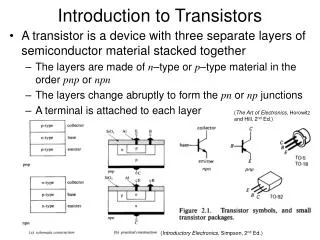
Introduction to MOS Transistors
Introduction to MOS Transistors. Section 6.1-6.4. Outline. Similarity Between BJT & MOS Introductory Device Physics Small Signal Model. BJT & MOS Transistor. [Chapter 4,5]. [Chapter 6,7]. Analogous Devices. Terminals “C”↔”D” “E” ↔”S” “B” ↔”G” Analogous Devices NPN ↔NMOS PNP ↔PMOS.

Introduction to MOS Transistors
E N D
Presentation Transcript
Introduction to MOS Transistors Section 6.1-6.4
Outline • Similarity Between BJT & MOS • Introductory Device Physics • Small Signal Model
BJT & MOS Transistor [Chapter 4,5] [Chapter 6,7]
Analogous Devices • Terminals • “C”↔”D” • “E” ↔”S” • “B” ↔”G” • Analogous Devices • NPN ↔NMOS • PNP ↔PMOS
A Crude Metal Oxide Semiconductor (MOS) Device V2 causes movement of negative charges, thus current. V1 can control the resistivity of the channel. Positive charge attract negative charges to the interface between insulator and silicon. A conductive path is created If the density of electrons is sufficiently high. Q=CV. P-Type Silicon is slightly conductive. The gate draws no current!
NMOS in 3D (provide electrons) (drain electrons) W n+ diffusion allows electrons move through silicon.
Typical Dimensions of MOSFETs These diode must be reversed biased. tox is made really thin to increase C, therefore, create a strong control of Q by V.
A Closer Look at the Channel Formulation Need to tie substrate to GND to avoid current through PN diode. VTH=300mV to 500 mV (OFF) (ON) Free electrons appear at VG=VTH. Positive charges repel the holes creating a depletion region, a region free of holes.
Change Drain Voltage Resistance is determined by VG.
Change Gate Voltage A higher VG leads to a lower channel resistance, therefore a larger slope.
Length Dependence fixed VD fixed VG The resistance of a conductor is proportional to the length.
Dependence on Oxide Thickness fixed VD fixed VG Q=CV C is inversely proportional to 1/tox. Lower Q implies higher channel resistance.
Width Dependence The resistance of a conductor is inversely proportional to the cross section area. A larger device also has a larger capacitance!
Channel Pinch Off • Q=CV • V=VG-VOXIDE-Silicon • VOXIDE-Silicon can change along the channel! Low VOXIDE-Silicon implies less Q.
VG-VD is sufficiently large to produce a channel VG-VD is NOT sufficiently large to produce a channel No channel Electrons are swept by E to drain. Drain can no longer affect the drain current!
Regions (No Dependence on VDS) No channel Assumption: