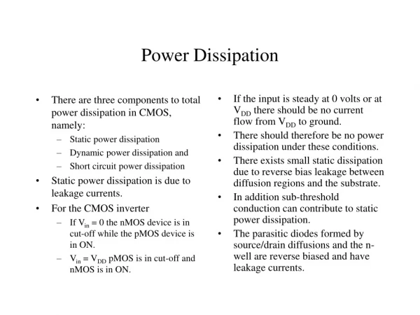
Download
1 / 24
240 likes | 268 Vues
Explore a novel charge pump-based receiver circuit to reduce interconnect power dissipation, enabling energy-efficient data transmission in next-generation computing systems. Compare design and performance with existing solutions. Save up to 70% energy in processor data buses. Achieve optimal power-performance-area (PPA) with this innovative interconnect circuit.

E N D
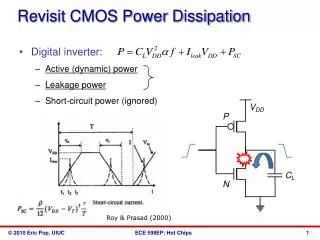
A Charge Pump Based Receiver Circuit to Reduce Interconnect Power Dissipation Aatmesh Shrivastava, John Lach, and Benton H. Calhoun University of Virginia, Charlottesville
Interconnect Power Dissipation [1] Magen, et. al. SLIP 2004 • Interconnect consumes >50% of dynamic power in a micro-processor. • 90% of interconnect power is in 10% of interconnect.
Interconnect Power in the context of next generation computing • A Exa-byte of data is to be transmitted per second to enable exascale computing. • [2] P. Kogge et. al. DARPA/ITPO 08 • State of the interconnect consumes 1-3pJ/bit/mm. A exabyte/s will need 10-30 Mega-Watt Power. [2]
Outline • Voltage Scaling for Interconnect • Driver • Receiver • Literature Review • Proposed Interconnect Receiver • Charge Pump • Complete circuit diagram • Simulation • Implementing the interconnect in 4 core Alpha • Results • Design Comparison
Voltage Scaling for interconnects • Voltage Scaling has been used to reduce interconnect power [4-10]. • Logic runs at rated VDD, wires at reduced VDDI. Interconnect driver circuits are needed • Key Question :- Performance overhead vs Power.
Interconnect Driver [4] H. Zhang, et. al. TVLSI 2000 • Two NMOS transistors are used at output stage • A signal at logic level ( 1V) is converted to a signal interconnect level (0.3V) • We use this driver in our proposed interconnect circuit.
Interconnect Receiver ON ON VDDI OFF 0 • Restores the signal back to the logic level. Poor performance, VDDI > VT. • Differential amplifier [8-10] can be used for better performance but have higher power overhead. • We propose an improved single ended receiver.
Approx. Power-Performance-Area Prior Art • In prior art either energy saving is less or performance is poor.
Delay vs Energy/bit : Prior Art • Existing solutions do not address power and performance in conjunction.
Proposed receiver ckt • Charge-pump is used. • It boosts the signal to three times the interconnect swing • Good performance and much lower power
Charge Pump in the Receiver • When IN is at 0, A is precharged to 0.3V. So when IN goes high A goes to 0.6V (Ideal case). • Similarly when IN is at 0.3V, A is precharged to 0V. So when IN goes low A goes to -0.3V (ideal). • Total swing at A is 0.9V. C swings from VT to VDD-VT
Complete Circuit Diagram VTL 0V 1V 0V 0.3V VDD-VTL -0.3 VTL 1 1 0.3 VTL VTL+0.3 0 0.6 0 VTL 0 0.3 0 0
Simulation results IN OUT • Reduced swing interconnect signal gets reconstructed with good performance.
Delay vs Energy/bit • Proposed Solution gives very good performance and very low energy.
Energy savings in a processor • Data-Bus of alpha was implemented using differential, basic and proposed interconnect circuit. • Over the set of splash benchmarks, the proposed interconnect saves up to 70% of energy.
PPA : Power-Performance-Area • Novel interconnect circuit has best in class PPA
References • NirMagen et. Al. “Interconnect-Power Dissipation in a Microprocessor” Workshop on System Level Interconnect Prediction 2004 • P. Kogge, K. Bergman, S Borka, et. al, “ExaScale Computing Study: Technology Challenges in Achieving Exascale Systems” DARPA/IPTO, September 2008 • E. Kusse and J.M. Rabaey, “Low-Energy Embedded FPGA Structures” IEEE International Symposium on Low Power Electronics Design, August 1998 . • H. Zhang, V. George and J.M. Rabaey, “Low-Swing On-Chip Signalling Techniques: Effectiveness and Robustness” IEEE Transactions on Very Large Scale Integration (VLSI), Vol-8 No-3, June 2000 • J.C.G. Montesdeoca, J.A. Montiel-Nelson and S. Nooshabadi, “CMOS Driver Receiver Pair for Low Swing Signalling for Low Energy On-chip Interconnects” IEEE Transactions on Very Large Scale Integration (VLSI), Vol-17 No-2, February 2009. • R. Ho, I. Ono, F. Liu, A. Chow, J. Schauar and R. Drost, “High Speed and Low Energy capacitively driven wires” IEEE International Solid State Circuits Conference, February 2007. • M. Ferretti and P.A. Beere “Low Swing Signaling Using a Dynamic Diode-Connected Driver” European Solid-State Circuits Conference, September 2001. • A. Narshimha, M. Kasotiya and R. Sridhar “A Low-Swing Differential signaling Scheme for on-chip Global Interconnects” International Conference on VLSI Design, January 2005. • N. Tzartzanis, W.W. Walker “Differential Current Mode Sensing for Efficient On-Chip global Signaling” IEEE Journal of Solid State Circuits, Vol-40 No-11, November 2005. • H. Ito, M. Kimura, K. Miyashita, T. Ishii, K. Okada and K. Masu, “A Bidirectional and Multidrop Transmission Line Interconnect for Multipoint to Multipoint On-Chip Communication” IEEE Journal of Solid State Circuits, Vol-43 No-4, April 2008. • V. Alder and E.G. Friedman, “Repeater Design to Reduce Delay and Power in Resistive Interconnects”. IEEE Transactions on Circuits and Systems-II, Vol-45 No-45, May 1998. • P.E. Allen and D.R. Holberg., “CMOS Analog circuit design” Oxford Press 2002. • R.E. Kessler, E.J. McLellan and D.A. Webb, “The Alpha 21264 Microprocessor Architecture” International Conference on Computer Design, October 1998. • N.L. Binkert, R.G. Dreslinski, L.R. Hsu, K.T. Lim, A.G. Saidi and S.K. Reinhardt, “The M5 Simulator: Modeling Networked Systems” IEEE Micro, July 2006.
Complete Circuit Diagram • When IN goes hi, A goes to 0.6V, bringing B to ground. • OUT goes high completing the transition. • It also brings C to VDD-VT and precharges A to 0.6V