Download
1 / 10
100 likes | 272 Vues
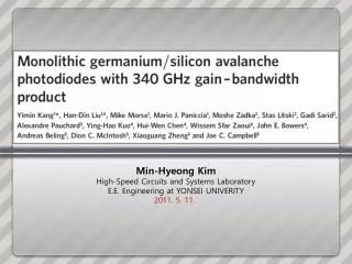
Min- Hyeong Kim High-Speed Circuits and Systems Laboratory E.E. Engineering at YONSEI UNIVERITY 2011. 5. 11. . [ Contents ]. Abstract Background SACM APD structure Ionization/multiplication coefficient Device structure Measurement results Dark current

E N D
Min-Hyeong Kim High-Speed Circuits and Systems Laboratory E.E. Engineering at YONSEI UNIVERITY 2011. 5. 11.
[ Contents ] • Abstract • Background • SACM APD structure • Ionization/multiplication coefficient • Device structure • Measurement results • Dark current • Excess noise factor & Gain-Bandwidth product • Receiver sensitivity & BER • Conclusion
1. Abstract • Monolithic Ge-Si SACM APD operating at 1300nm • (separate absorption, charge and multiplication avalanche photodiodes) • Gain-BW product : 340GHz • K_eff : 0.09 • A receiver sensitivity • : -28dBm at 10Gb/s • Si material properties allow for high gain with less excess noise than InP-based APD and a sensitivity improvement of 3dB or more. • With Si, an even higher gain–bandwidth product could be achieved based on a simple layer structure with relatively large process tolerances.
2. Background • Ⅰ. SACM APD (separate absorption, charge and multiplication APD) InAlAs-based APDs (Ref.17) InAlAs-based APDs (Ref.18) Si-based APDs (This work)
2. Background • Ⅱ. Ionization/Multiplication coefficient • K : Ratio of the ionization coefficients of electrons and holes. • A low k value is desirable for high-performance APDs. Impact Ionization probability = Multiplication coefficient M → Excess Noise factor F(M)
3. Device structure • SACM APD • Punch through voltage -22V • Breakdown voltage -25V with Responsivity 5.88A/W Designs for a floating guard ring (GR) with various distances (1–3 mm) between the guard ring and the mesa edge were introduced to reduce the surface electric field strength at the silicon/insulator interface to prevent premature breakdown along the device perimeter.
4. Measurement results • Ⅰ. Dark current • When the reverse bias increase, not only the gain becomes large but also the dark current increases. • It is because of (1) junction leakage current (generation and recombination) and (2) tunneling current. • The breakdown voltage is -25V, and here at the dark current of 10uA. • All these measurements are supported at 1300nm wavelength.
4. Measurement results • Ⅱ. Excess noise factor • & Gain-Bandwidth product F(M) • After measurement of excess noise factor, the k value is calculated about to 0.09 by using above equation. • All measured devices had a gain–bandwidth product over 300 GHz. The highest gain–bandwidth product obtained was 340 GHz. • The 3dB BW was measured using Agilent 8703A Network Analyzer. The bandwidth is limited by RC and transit time effect. • As the gain is increased beyond 20, the bandwidth dropped owing to the avalanche build-up time effect.
4. Measurement results A gain of 10 & -20dBm input optical power • Ⅲ. Receiver sensitivity & BER • APD+TIA+CDR for BER measurement • A data rate of 10Gb/s • Using a pseudo-random binary sequence(PRBS) and extinction ratio(ER) of 12dB. • In this set, the input optical power(Receiver sensitivity) was maximun-28dBm. ** Sensitivity in a receiver is normally defined as the minimum input signal Si required to produce a specified signal-to-noise S/N ratio. (So, it is a function of the SNR or BER.)
5. Conclusion • To improve more, • Reducing the dark current of the APDs. • : Better control of the germanium profile with respect to the electric field distribution in the device can reduce the tunneling current. • (2) Reducing the value of k_eff. • : Studies have shown that k_eff can be reduced by optimizing the multiplication region thickness. By this, we believe that a sensitivity of approximately -32 dB m could be achieved. • Demonstrate a monolithically grown, CMOS-compatible Ge-Si SACM APD device with a gain–bandwidth product of 340 GHz and a k_eff of 0.09 at 1300nm wavelength. • The optical receivers built with this Ge-Si APDs demonstrated a sensitivity of -28 dBm at 10Gb/s.