Paging in 80386 Memory Management Unit
Learn how Paging enhances memory management in 80386 MMU, its optional usage, support registers involved, page descriptors, and advantages. Explore page directory, table entries, and control mechanisms for efficient memory utilization.

Paging in 80386 Memory Management Unit
E N D
Presentation Transcript
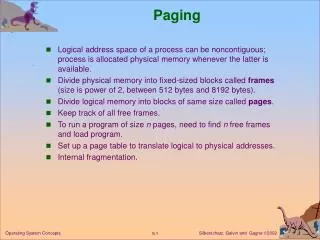
Paging • The internal Memory Management Unit (MMU) of 80386 can be used to add another level of indirection to the existing segmentation and protection mechanisms. The technique for doing this is known as ‘Paging’. • The use of paging feature is optional & it is not available with real mode operation of 80386. • Paging is beneficial in a multi-user system, in an open architecture, bus structured system. • The paging MMU works beneath the segmentation MMU & it augments rather than replaces segmentation mechanism. • When paging is disabled, the 4 Gb physical address space is organized into segments that can be of any size from 1 byte to 4 Gb. Processor Architecture and Interfacing
However, when paging is enabled the paging unit arranges the 4 Gb physical address space into 1048496 (1 M) pages that are each 4096 bytes (4 Kb) long as shown in the figure. • The fixed size blocks of paged memory are disadvantageous as 4 K addresses are allocated even though not all of them are used. This creation of unused sections of memory is called fragmentation, which results in less efficient use of memory. Processor Architecture and Interfacing
Support registers • Following registers are used by the 80386’s paging mechanism. Processor Architecture and Interfacing
Various control registers used in paging are – CR0, CR2 & CR3. • In CR0, the MSB (bit 31) i.e. PG is used to control the paging operation. If the PG bit is set, it enables the paging operation (paging MMU) otherwise paging is disabled. • CR2 is a read only register. During the page translation mechanism if the page fault occurs then 80386 saves the address at which the page fault occurred into CR2 register. This address is known as page fault linear address. • CR3 (most significant 20 bits) is also known as page directory base register (PDBR) & holds 20-bit page directory base address which points to the start of page directory which is 4KB aligned. Processor Architecture and Interfacing
Descriptors • Paging requires 2 types of tables: page directory & page tables. Both types are made up of 32 bit (4 bytes) descriptors. • Each page directory & page table contain exactly 1024 descriptors. Therefore, size of them is 4096 bytes (4 kB) each. • A descriptor in a page directory is known as page directory entry (PDE). Also, a descriptor in a page table is known as page table entry (PTE). • The format of PDE & PTE is shown in next figure. Processor Architecture and Interfacing
PDE descriptor • Page table address: The most significant 20 bits of PDE point to the base of a page table. It is a physical address. The least significant 12 bits of this address are all 0s. • User: Bits 9, 10 & 11 are not used by 80386. Programmer can use them as he/she wish. • Accessed: 80386 automatically sets the bit 5 (A) whenever this PDE is used in address translation. • User/Supervisor: Bit 2 is U/S protection bit. If this bit is set the memory pages that this PDE covers are accessible from all privilege levels. If it is cleared the pages are accessible only by PL 0, 1 & 2 (supervisor) code. Processor Architecture and Interfacing
Read/Write: Bit 1 is R/W protection bit. If U/S bit is clear this bit has no effect. If U/S bit is set, this bit determines whether the pages covered by this PDE are write protected or not. If R/W = 1 write operation is allowed otherwise not. • Present: Bit 0 is P bit. If this bit is set the page table pointed by this PDE is present in physical memory. • If P bit is clear, the page table is not present in physical memory & the rest of this PDE is available for use by programmer. The format of not present page descriptor is as shown in earlier figure. Processor Architecture and Interfacing
PTE descriptor • Page frame address: The most significant 20 bits of PTE point to the base of a page frame or simply page. It is a physical address. The least significant 12 bits of this address are all 0s. • User: Bits 9, 10 & 11 are not used by 80386. Programmer can use them as he/she wish. • Accessed: 80386 automatically sets the bit 5 (A) whenever this PTE is used in address translation. • User/Supervisor: Bit 2 is U/S protection bit. If this bit is set the memory page that this PTE covers is accessible from all privilege levels. If it is cleared the page is accessible only by PL 0, 1 & 2 (supervisor) code. Processor Architecture and Interfacing
Read/Write: Bit 1 is R/W protection bit. If U/S bit is clear this bit has no effect. If U/S bit is set, this bit determines whether the page covered by this PTE is write protected or not. If R/W = 1 write operation is allowed otherwise not. • Present: Bit 0 is P bit. If this bit is set the page pointed by this PTE is present in physical memory otherwise not. • Dirty: Bit 6 is D bit. It is automatically set by 80386 whenever the page frame which this PTE covers is written into. Processor Architecture and Interfacing
Segmentation Vs. Paging Processor Architecture and Interfacing
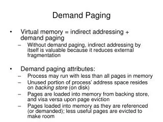
3 Major Capabilities of Paging hardware • Address Translation • Page Translation converts 32 bit linear address To 32 bit physical address transparently to add one more indirection to suit your particular needs. • Page level Protection • This feature can only be used to make access more restrictive. They cannot loosen permissions already denied by the segmentation. • Demand Paging ( Virtual Memory ) • Used for virtual memory management. Virtual means being in effect but not in fact. • Creates illusion of infinite memory by using primary memory as cache between processor & secondary memory – Based on principle of locality Processor Architecture and Interfacing
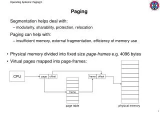
1. Address translation • The segmentation & paging mechanism convert 48 bit logical addresses into 32 bit physical addresses required by the hardware. • The block diagram of address translation is shown in the next figure. • At first, the segment translation is performed on the logical address. Then if paging is disabled, the linear address produced is equal to the physical address. • However, if the paging is enabled, the linear address goes through a second translation process, known as page translation, to produce the physical address. Processor Architecture and Interfacing
Paging is advantageous as it greatly simplifies the implementation of the memory manager software. • As shown in figure, the linear address produced by the segment translation is not used as physical address, as it undergoes a second translation called the page translation. • The format of the linear address is as shown in earlier figure. It has 3 fields: 12 bit offset field, 10 bit page field & 10 bit directory field. Processor Architecture and Interfacing
Page Translation Processor Architecture and Interfacing
Linear Address Format • TLB (Translation Lookaside Buffer) • maintaining 32 sets of table entries • 128 KB of paged memory are always directly accessible DIR PAGE OFFSET 31 22 21 12 11 0 Page Frame Operand Translation lookaside buffer (TLB) Page table entry Page table Page directory entry Page directory table PDBR(CR3)
The translation of linear address 00C03FFCH to physical memory address XXXXXFFCH. The value of XXXXX is determined by the page table entry (not shown here). Processor Architecture and Interfacing
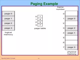
The diagram, shows how a linear address is translated into its equivalent physical address. • The address in the page directory base register (PDBR) in CR3 locates the page directory table in memory. This address is 32 bits long. The upper 20 bits are from the CR3 & the lower 12 bits are assumed to be 000 H at the beginning of the directory & range to FFF H at its end. • Therefore, the page directory is of size 4 K. It consists of 1K, addresses each of size 32 bit. These addresses each point to a separate page table. • The 10 bit directory field of the linear address is the offset from the start of the page directory table & selects one of 1K entries. • This pointer (32 bit address) of the desired page table is cached into translation look- aside buffer (TLB). Processor Architecture and Interfacing
This value is used as the base address of a page table in memory. • Each page table is also 4 Kb long & contain 1K, 32 bit addresses. These addresses are called page frame addresses. Each page frame address points to a 4 K frame of data storage locations in physical memory. • The 10 bit page field, of the linear address selects one of the 1K, 32 bit page table entries & is cached into TLB. • This frame of memory locations is used for storage of data. The 12 bit offset part of the linear address identifies the location of the operand in the active page frame. • The TLB is capable of maintaining 32 sets of table entries. So 128 Kb of paged memory is always directly accessible. Operands in this part of memory can be accessed without first reading new entries from the page table. Processor Architecture and Interfacing
TLB Testing • When TLB testing is to be performed Paging must be turned OFF • Test Registers TR6 & TR7 are used Fig - TLB Structure • Structure of TLB • Four way set associative cache • 4 sets of 8 entries each • Each entry consists of TAG (24 bits) & DATA (20 bits) • TAG contains valid bit, 3 attribute bits – D, U/S & R/W & & high order 20 bits of linear address DATA contains high order 20 bits of physical address Processor Architecture and Interfacing
Test Registers • TR6 – Test Command register • TR7 – Test Data Register • Test Registers are privileged resources & so can be accessed from PL 0 code only. Processor Architecture and Interfacing
TR6contains a command & addr tag to use in performing the command Processor Architecture and Interfacing
TR6 Processor Architecture and Interfacing
TR7Holds data read from or written into TLB Processor Architecture and Interfacing
TLB Operations Processor Architecture and Interfacing
2. Page level protection • The least significant 3 bits (i.e. P bit, U/S bit & R/W bit) of the PDE & PTE are used in page level protection. • These bits are explained in detail next. Processor Architecture and Interfacing
P bit • If P bit of PDE is cleared & 80386 tries to use this PDE, it will generate a page fault (exception 14). The paging function will be aborted, no memory will be accessed, & control will be transferred to page fault handler. • Thus, if P bit is not set, 80386 will never be able to access any of the 1024 PTEs of the page table to which this PDE points. • When there are holes in the linear address space & user intentionally wants to omit that portion of memory, it is recommended to clear the P bit. • The use of P bit in PTE is very similar to that of P bit in PDE but on a smaller scale. Processor Architecture and Interfacing
U/S bit • If U/S bit of PDE is cleared the 4 Mb physical space pointed by this PDE is accessible only to programs running at the supervisor level. • Thus, one can deny access of the physical space even if the segmentation mechanism & segment level privilege protection allows it. • The use of U/S bit in PTE is very similar to that of U/S bit in PDE but on a smaller scale. (4 kB memory space.) • If U/S bits in PDE or PTE cause a privilege violation the processor will generate a page fault (exception 14). The paging function will be aborted, no memory will be accessed, & control will be transferred to page fault handler.. Processor Architecture and Interfacing
R/W bit • Bit 1 of PDE or PTE sets read/ write permission for a 4 MB block or 4 KB page frame respectively. • This bit has an effect only if U/S = 1 i.e. read write permission does not apply to supervisor level programs. • In a PDE, if U/S =1 & R/W =1 all privilege levels can freely read & write into the physical space pointed by PDE. If R/W = 0, write permission is not allowed to PL 3 code. • If a program attempts to write in such area, it will generate a page fault (exception 14). The paging function will be aborted, no memory will be accessed, & control will be transferred to page fault handler. Processor Architecture and Interfacing
3. Demand Paging (Virtual memory Management) – 5 Step Process • Step 1- Determining Memory requirement • To Know when program has requested nonexistent memory P bit in PDE/PTE, Page fault, PF handler • Step 2 – Allocating Memory • Uses LRU algorithm to select a page for replacement • Step 3 – Saving the contents of Reallocated memory • Contents of a page to be replaced is copied into swap devices conveniently hard disk drives if required (which can be determined by reading status of D bit in PTE) to save time since it is time expensive. Processor Architecture and Interfacing
3. Demand Paging (Virtual memory Management) – 5 Step Process • Step 4 – Remapping a page of memory • a. Clearing P bit of PTE for a page selected for replacement • b. Changing PTE which generated page fault by changing 20 bit page frame address to point to the physical base address of the page frame & setting P bit • Paging cache (TLB) need to be flushed & reloaded • Program is restarted through IRET • Step 5 – Restoring Reallocated Pages • If program makes a JMP or CALL to the code that was mapped out in step 3 then again page of physical memory need to be selected to allocate to the hole in linear address Space & swap out that if necessary & finally retrieving the contents Processor Architecture and Interfacing
Entering into PM • 80386 requires a very complex data structure to operate in protected mode. • After power on or reset operation, 80386 enters into real mode of operation because it requires systems programmer to set up many complex table required for PM operation. • Technically the 80386 begins operating in PM when PE bit in CR0 is set by software. However practically there is much more to do for proper switch from RM to PM. • Flowchart for switching from RM to PM is shown in next figure. Processor Architecture and Interfacing
80386 at start performs a self test. • If there is no error in executing the self test (i.e. content of AX = 0) then it checks for numeric coprocessor is installed or not? (i.e. ET bit of CR0). • Check ET bit in CR0. If ET = 1 then set MP bit of CR0. (Either 80387 or 80387 is installed). Otherwise it set EM i.e. software emulator is used to perform numeric operations. • Initialize all data segments (DS, ES, FS, GS) & then stack segment (SS, SP). • Now, copy GDT & IDT from ROM to RAM & loads their staring address in GDTR & IDTR respectively. • Also copy page tables & TSSs from ROM to RAM. • Now set the PE bit. Processor Architecture and Interfacing
Returning back to RM • To return the processor to real mode without turning off the power & resetting the system, one needs to clear the PE bit in CR0. • Before this, if paging is enabled, one needs to disable it by clearing the PG bit in CR0 & also zero out CR3 so that the paging cache will be cleared. • Next is to use segment descriptors that look like real mode segments. For this load selectors which will point to the descriptors with the attributes shown in table into all four data segment registers & stack segment register. • Also load CS with selector to a code descriptor having these attributes except for writable attribute using the FAR JMP instruction. Processor Architecture and Interfacing
FAR JMP instruction will also flush the 80386’s instruction prefetch queue. • 80386 is now operating in real mode. Flowchart shown next outlines the procedure for disabling the protected mode. Processor Architecture and Interfacing
Multitasking • A task can be a single program or it can be a group of related programs. • A multi-user system also implies multitasking but reverse is not true. • In multitasking operation, 80386 is actually serving only one task/user for a short time & then moving onto the next task/user & so on. Each task/user is allotted a time slice (a small fraction of second) . • When the current task/user has used up its time slice, the 80386 saves all of the current context information & directs towards next task/user. Processor Architecture and Interfacing
After serving all tasks/users, 80386 will return to the first task/user , pick up where it left off & do as much work as it is able in a time slice. • This technique is known as timesharing. Processor Architecture and Interfacing
Task State Segment • A task can be a single program or it can be a group of related programs. • In 80386, a task is any collection of code & data that has a Task State Segment (TSS) assigned to it. It is where the 80386 stores a task’s vital information when the task is not running. It is also where 80386 finds all of the information necessary to restart that task when its turn comes again. • TSS is an area of read/write memory like data segment which is not accessible to the general user program even at PL0. • The space defined within a TSS is available to 80386 only. • Format of TSS is shown in next figure. Processor Architecture and Interfacing
I/O map base Processor Architecture and Interfacing
TSS descriptor • The TSS is defined by a segment descriptor which is known as TSS descriptor. • It appears only in GDT. • The format of TSS descriptor is shown below. Processor Architecture and Interfacing
The base address field determines the starting address of TSS. • The limit field determines the size of TSS. As 80386 requires 104 bytes of storage in order to perform a context save, the limit field must never be less than 00067H. • The DPL field does not imply a privilege level for the TSS itself. It determines what software can reference the task defined by this TSS. Processor Architecture and Interfacing
Task register • It is a key element in the protected mode task switching mechanism of the 80386. • It holds the 16-bit selector. The initial selector must be loaded into TR which starts the initial task. The selector is changed automatically whenever the 80386 perform a task switch. • As shown, the TR is used to locate a descriptor in the GDT. The corresponding task state segment (TSS) descriptor gets automatically read from the global memory & is loaded into task descriptor cache. • This descriptor defines TSS & provides the starting address (BASE) & the size (LIMIT) of the present segment. • Every task has its own TSS which holds the information needed to initiate the task. Processor Architecture and Interfacing
Task Gate Descriptor Processor Architecture and Interfacing
Task Gate Indirectly identifies a task Processor Architecture and Interfacing
Task Switching Processor Architecture and Interfacing
Task Switching Operation – 5 steps Processor Architecture and Interfacing