Download

1 / 10
100 likes | 232 Vues
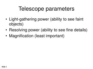
What is Helsinki Silicon Beam Telescope?. Helsinki Institute of Physics (HIP) has operated the Silicon Beam Telescope (SiBT) at the CERN H2 test beam area since 1990.

E N D
What is Helsinki Silicon Beam Telescope? • Helsinki Institute of Physics (HIP) has operated the Silicon Beam Telescope (SiBT) at the CERN H2 test beam area since 1990. • SiBT has eight (8) position sensitive silicon strip detectors with appropriate front-end electronics and data acquisition system • SiBT is a unique detector testing unit for testing novel full-size particle detectors(resolution, efficiency, and signal-to-noise ratio). Picture 1: Old SiBT SiBT will be completely updated for the summer 2007 beam tests ! Panja Luukka
Motivation for the SiBT update • Novel radiation hard detectors are being developed for Super-LHC, and LHC Council requires tests on full-size detector systems. • Other CERN detector groups have inquired possibilities to test their detectors with our beam telescope. • SiBT and our other unique testing unit Finnish Cosmic Rack (FinnCRack) reinforce each other., especially after the upgrade. Picture 2: Teppo Mäenpää working with FinnCRack at HIP Helsinki Laboratories Picture 3: HIP students installing cables for SiBT at H2 Panja Luukka
SiBT mechanics • Existing: • Component 1: stone base • 2: support rail • Need to be built: • 3: support frame for detector enclosures • 4: detector enclosures • 5: detector encloseure with cooling • 6: cover plate • 7: attachment system for front-end electronics • 8: support for scintillators • 9: scintillators • 10: photomultipliers Picture 4: SiBT Mechanics. Picture by Erkki Anttila. Note: real directions of the scintillators are perpendicular instead of parallel Panja Luukka
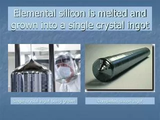
SiBT detectors • Detector processing will be done at the clean room of Helsinki University of Technology Microelectronics Centre • Material is Float Zone 4” n-type silicon wafers obtained from CERN RD50 (depleted at 50 V) • Litography masks are designed so that two 4 cm * 4 cm detectors will be obtained from one wafer • Other detector measures: • Pitch 50 um • 768strips per detector (=6*128) • Suitable for a CMS 6-APV chip Picture 5: Esa Tuovinen processing silicon detectors at Helsinki University of Technology Microelectronics Center Panja Luukka
SiBT front-end electronics • Hybrids • We need at least 8 hybrids + 4 spares, currently we have 5 hybrids • Bonding • at CERN detector laboratory? • Pitch Adapters • Needed between detector and APV-hybrid, layout already done Picture 6: CERN RD39 silicon detector module with APV-hybrid. Picture 7: Example of the pitch adapter layout made by Layed-program Panja Luukka
SiBT cooling • Design based on a cooling box with Peltier –element and chiller • Minimum temperature of the detector inside the box will be – 16ºC. • Humidity inside the box will be about 30 %, flushed by dry nitrogen • Based on Thermo Electric Cooler • Cooling box will be easily opened and non-hermetical Picture 8: Cooling box containing the detector under tests attached to SiBT during the summer 2004 beam tests Panja Luukka
SiBT trigger system and voltage sources • Trigger system: • Incl. 2 scintillators, 2 photomultipliers, 2 discriminators • Incl. 5 shapers, 1 coincidence unit • Power supplies control and monitor electronics • Low Voltage Power Supplies • 10x 2.5V/3A and 1,25V/2A fast reacting PVs with voltage and current monitors • High Voltage Power Supplies • For reference detectors 8x 0-100V/2mA PVs with voltage and current monitors • For the detector under investigation the power supply will provide up to 1000 V Picture 9: Dr. Sandor Czellar beside four high voltage power supplies and a trigger box he has developed and manufactured for the Finnish Cosmic Rack. Similar PVs and Trigger Systems are used in CMS Tracker module testing centers. Panja Luukka
SiBT data acquisition • The SiBT DAQ will be updated to be similar to that of the CMS Tracker • The major difference is that electrical front-end drivers (FED) will be sufficient. • We have most of the readout components (1 FED, 1 tracker readout interface, communication and control unit, front-end controller, trigger and sequencer card) • but we would still need for the telecope readout: • 2-3 electrical FEDs • tracker readout interface schematics • More APV-hybrids Picture 10: SiBT Data Acquisition will be similar to that of CMS Tracker Panja Luukka
Cost Estimate for the SiBT Update Panja Luukka
Conclusions • We would appreciate if you have any comments or suggestions concerning the design etc. of the telecope. • In order to provide this tool for the full size detector characterization, we also would be happy to get help in: • getting certain components such as the APV-hybrids, FEDs etc. • in the software development e.g. if you have students, who would like to get hands-on experience in the software development of a DAQ or online/offline analysis. Panja Luukka