### Technical Design Overview of the Forward Vertex Detector Electronics and DAQ Readout System ###
120 likes | 258 Vues
This document details the technical design specifications for the Forward Vertex Detector's electronics and DAQ readout system, composed of two main parts: the Readout Chip (ROC) and the Front-End Module (FEM). The ROC manages data compression and serialization near the detector, employing radiation-tolerant FLASH-based FPGAs and transmitting data via fibers. The FEM buffers data for up to 64 beam clocks, combining input from multiple ROC channels, and communicates with the Data Collection Module (DCM). The design ensures flexibility, programmability, and synchronization essential for high-frequency data processing. ###

### Technical Design Overview of the Forward Vertex Detector Electronics and DAQ Readout System ###
E N D
Presentation Transcript
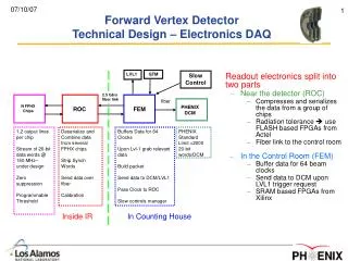
Forward Vertex DetectorTechnical Design – Electronics DAQ Readout electronics split into two parts • Near the detector (ROC) • Compresses and serializes the data from a group of chips • Radiation tolerance use FLASH based FPGAs from Actel • Fiber link to the control room • In the Control Room (FEM) • Buffer data for 64 beam clocks • Send data to DCM upon LVL1 trigger request • SRAM based FPGAs from Xilinx LVL1 GTM Slow Control 2.5 Gb/s fiber link fiber N FPHX Chips FEM PHENIX DCM ROC 1,2 output lines per chip Stream of 20-bit data words @ 150 MHz– under design Zero suppression Programmable Threshold Deserialize and Combine data from several FPHX chips Strip Synch Words Send data over fiber Calibration Buffers Data for 64 Clocks Upon Lvl-1 grab relevant data Build packet Send data to DCM/LVL1 Pass Clock to ROC Slow controls manager PHENIX Standard Limit <2000 20-bit words/DCM Inside IR In Counting House
Data Word structure TBD FPHX Chip Design Reminder • Based upon well tested FPIX2 chip design • Data push readout over 2 output lines • Zero suppression with programmable threshold • Fully programmable logic with masking capabilities • Data contains: • 3 bit ADC • 7 bit Strip Information • 6 bit Beam Counter • 26 chips/large wedge, 12 chips/small wedge • 2(4) wedges (52 chips)-->ROC channel • 16 wedges-->ROC board Time (ns)
ROC Design Specifications • Generate ~130 MHz Serializer Clock • Provides Control, Download and Calibration signals for the chips • Combine serial data from 52 FPHX chips ( 2 wedges) (partially) • Synchronize readout and strip off Sync Words • Append CHIP ID to the data • Send parallel data word output at 130 MHz over 2 fiber interface to the FEM • Move from ACTEL A3PE600 to ACTEL A3PE3000 FLASH based FPGA = done
ROC To Do/Plans • Needs full testing with multiple chips, multiple readout lines • Proper data packaging for serdes/FEM (not sure if this is complete) • Finish specifications so that prototype layout can be completed (especially pin-out needed). Can be started already. • ACTEL chip with enough I/O for full production will be tested with prototype board • Connect to FEM with fiber-driver
8-chip module USB Interface DigiIO Actel Board ROC Prototype R&D • Actel A3PE600 prototype board • Slow control via USB interface (DLP-2232M) • Output data via NI-6534 PCI card at 20 MHz (up to 640 Mbps) • Test an 8-chip FPIX module (FPIX is progenitor of FPHX chip and has similar digital backend)
8-chip module USB Interface DigiIO Actel Board ROC Prototype R&D Covers 30 deg (16 wedges)
FEM Design Specifications • FEM receives data from a single ROC channel over two fibers at fixed rate of 2.5 Gbits/s • Main functionality • Store the data by BCO counter • Buffer data for 64 BCO clocks • Read the data from certain clock to output buffer at 300 MHz • Send the output buffer content to the DCM (partially) • Plan to combine the data from 4 FEM channels on single FEM board • Implementation • Xilinx mid-scale Virtex-4 FPGA VC4VSX35 • Use built-in FIFOs and Relationally Placed Macros (RPMs) for maximum performance and predictability (Provided by XILINX) = done
FEM To Do/Plans • Combine the data from 4 FEM channels on single FEM board • Get fiber transceivers working and connect ROC and FEM • Connect to PHENIX-type DAQ to check DCM compatibility: mini-DAQ? Or just use other computer connections and check data format? • Develop user-friendly computer interface. • DAQ should be ready then for various test stands, etc.
FEM R&D • Design tested with single chip readout and “fake” data and running chip calibration chain • 100% of hits propagates through FEM with realistic triggered readout • Readout to PC tested at 640 Mb/s rate using NI-6534 readout board Virtex-4 test board FPIX Chip
Test of Calibration System • Test each pixel by injecting 64 pulses at gradually increasing amplitude • Upper figure shows histogram of turn-on curve for one channel • Lower figure shows noise • Inject capacitor = 3fF Noise ~ 102 e
Transceiver Boards • Transceiver boards available now • Loop-back tests and some two-board tests working • Understanding clock, power-up sequence, requirements/sensitivities • Expect to make connection between ROC and FEM boards relatively soon, but want to explore long-term operation/stability of fiber drivers in some detail
System Test Plans • Would like to get a mechanical setup which can hold one or several wedges designed and built relatively soon • Option for source tests, cosmic tests, beam tests(?) • Determine user-friendly DAQ interface, which can be multi-purpose (?) (above tests, QA tests, …) • Layout of LDRD ROC and FEM boards started, plan to have working boards by Jan.