Download
1 / 29
310 likes | 1.08k Vues
11 . Opto-electronic Circuits and Multistage Amplifiers Design. 11.1 Opto-Electronics Circuits and Design 11.2 BJT Cascode Amplifier and Design 11.3 BJT Phase Splitter and Design 11.4 BJT Direct Coupled Amplifier and Design 11.5 BJT Transformer Coupled Amplifier and Design .

E N D
11. Opto-electronic Circuits and Multistage Amplifiers Design 11.1 Opto-Electronics Circuits and Design 11.2 BJT Cascode Amplifier and Design 11.3 BJT Phase Splitter and Design 11.4 BJT Direct Coupled Amplifier and Design 11.5 BJT Transformer Coupled Amplifier and Design
11.1 Opto-electronics Circuits and Design Fundamentals of Photo-electricity If the electricity in a device changes due to the luminous power coming from the light, the device is called “ Photo-electric device “. Photo-resistor, Photo-diode, Photo-transistor, Opto-couplers are all Photo-electric devices. Photo-electric relationships According to the photo-efficiency of the type of the lamp, PV usually is very small and it is between 1 % to 3 % of the electrical power. The rest is the heat power PH which is 97 % to 99 % of the electrical input power.
Electrical power W = V*I = PV +PH where luminous power PV=h W and heat power PH=(1-h ) W taking h = photo efficiency of the light source If we assume that the light source is isotropic (radiating in all directions) having a sphere of radius “r” producing a surface area of 4pr2 , then the luminous power per unit area ( expressed in “E” ) will be: Fundamentals of Photo-diode Photo diode is reversed bias so that ID = 0 when no light falls ( E = 0 ) on it. More power from the lamp (either lamp nearer to diode or more electrical power to the lamp) will result more luminous power on the diode called E2 and E3 and so on, the reverse diode current will increase. In this way we will have different ID from different luminous power E.
Analysis and design of photo-diode circuits 1.Locate VS , 2.Locate ID=VS /R , 3.Find Q point at the crossing of E and R , 4.Read VD1 and ID1
Design Example Draw the photo diode circuit, sketch the load-line graph and design the value of “r” ( distance between lamp and photo-transistor), to produce VR = 10 V, if Photo-efficiency = 3 % ,VS = 20 V, R = 470 , and the lamp electrical power is 40 watts.
IC E1 VC Fundamentals of Photo-transistors The photo transistor is forward biased and has it’s Base sensitive to the light. The luminous power E falling on it’s Base will make the photo transistor to conduct producing IC. More luminous power E will result more collector current IC.
Analysis and design of photo-transistor circuits 1.Locate VCC, 2.Locate IC=VCC/R , 3.Find Q point at the crossing of E and R , 4.Read VCEQ and ICQ
Design Example Draw the photo transistor circuit, sketch the load-line graph and design value of R if “r” ( distance between lamp and photo-transistor) = 10cm, VR = 10 V, Photo-efficiency = 3 % ,VCC = 20 V, and the lamp electrical power is 40 watts.
Analysis of photo-transistor driven Comparator circuits photo-transistor driven comparator circuits (a) When there is no light E=0 , IC=0 V1 = 0. But V2 = 7.5V and because V1<V2 (less positive voltage going into negative terminal of comparator). then the output Vo will become positive and equals +13V. (b) The luminous power E falling enough on it’s Base will make the photo transistor to conduct producing IC. Then IC RE drop = V1 > V2, then the output Vo will become negative and equals -13V (c) Design condition is that enough luminous power E should make IC RE drop = V1 > 7.5V to have a negative voltage output at the comparator.
Analysis of photo-transistor driven Schmitt Trigger circuits • Here V1 should be greater than +6.5V. To make output Vo negative and equals -13V. • Here V1 should be less than -6.5V. To make output Vo positive and equals +13V. • The luminous power E is responsible to produce IC so that IC RE drop will make the Schmitt Trigger output either negative or positive, with a Hysterisis of ±6.5V
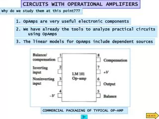
Fundamentals of Opto-couplers OPTO-COUPLERS are also called Opto-isolators. Inside the opto-coupler, light from LED excite the photo-transistor to flow collector current. The distance between LED and Photo device = r is fixed inside the IC and so the input and output characteristics of Opto-couplers are given by LED current IF versus current of the Photo device Ic or ID or IR depending upon which type of coupler is used.In the case of Photo-transistor couplers , input is IF and the output is Ic . Then we have a current gain between the input and the output called hF given by :-
Analysis and design of opto-coupler circuits 1.Locate VCC, 2.Locate IC=VCC/R , 3.Find Q point at the crossing of IF and R , 4.Read VCQ and ICQ
Design Example Draw the opto-coupler circuit, sketch the load-line graph and design the value of IF if hF = 0.5, VR = 10 V, VCC = 20 V, R = 1kW. What is the value of VCQ?
Analysis of Opto-coupler driven Schmitt Trigger circuits • Here V1 should be greater than +4.33V. To make output Vo negative and equals -13V. • Here V1 should be less than -4.33V. To make output Vo positive and equals +13V. • The Input LED current IF is responsible to produce IC so that IC RC drop will make V1 = ± 4.33V and the Schmitt Trigger output will become either negative or positive, with a Hysterisis of ± 4.33V
Summary of Design Equations Optical-Electronics Circuit and Design
Multistage amplifier consists of two or more amplifiers where the load on the first amplifier is the input of the second amplifier and so on. 11.2 BJT Cascode Amplifier and Design CE–CB Cascode amplifier
Assume RX+RY=R2 Both IB negligible or IB<<IRX RX design equation RY design equation CE-CB Cascode amplifier Cascode amplifier consists of two amplifiers using a single power supply VCC for both stages. The load on the first amplifier is the input of the second amplifier and so on. For Cascode amplifier, dc design is the same as before except design for RX and RY
IL Iin Ro Ri2 AV1 AV2 AVT Cascode amplifier ac design is made from the followings ac properties:
IL Base 2 Iin RX design equation RY design equation Summary of Design Equations CE-CB Cascode Amplifier ac Design Equations dc Design Equations
No ac condition Design Example Draw and design a Cascode amplifier for the following specifications: VCC = 12V, b = 200 (both), RE = 100W, RC = RL =2kW.Optimum IC condition
When the input to the amplifier is at Base and the output of the amplifier is at Emitter and also at Collector, the BJT amplifier is called Phase Splitter. • Two outputs of the Phase Splitter areopposite in phase, which is the most important property of this amplifier. It has the following ac circuit properties. Refer to CE with RE and EF analysis. 11.3 BJT Phase Splitter and Design Voltage gain-1 Voltage gain-2 Input resistance Output resistance-1 Output resistance-2 Current gain
IL1 IL2 Summary of Design Equations BJT Phase Splitter Amplifier
Design Example Draw and design the Phase Splitter with RL = 2kW, VCC = 20V, b = 200. Calculate Vo(pp) and Find Rin,Ai1 and Ai2 of your amplifier.
When the output and input of cascaded amplifier is directly connected without coupling capacitor, to improve lower cutoff frequency response, the amplifier is direct coupled amplifier. • Most important property of this amplifier is the dc conditions at the output is the same as dc conditions of the following amplifier input. Analysis and design may need better attention. Refer to CE with RE and EF analysis and take VC1=VB2 11.4 BJT Direct Coupled Amplifier and Design Voltage gain Input resistance Output resistance Current gain
Summary of Design Equations Direct Coupled Amplifier
Design Example Draw and design R1 and R2 of the Direct coupled amplifier with RC = 4kW, RE2 =RL= 4kW, Rin = 5kW ,VCC = 10V, b = 200(both BJT). AVT = -20. and Vo(pp)= 8V.
11.5 BJT Transformer Coupled Amplifier and Design • When the output of the amplifier is coupled to the load by using transformer, (to isolate dc into the load), the amplifier is transformer coupled amplifier. The circuit is shown with transformer coupled input. • Refer to CE with RE and take equivalent RC = n22RL Voltage gain Input resistance Current gain
Summary of Design Equations Transformer Coupled Amplifier
Design Example Draw and design R1 and R2 of the Transformer coupled amplifier with RL = 500W, RE = 500W, Rin = 5kW ,VCC = 10V, b = 200, n1 = 1, n2 = 2. Find the current gain Ai = iL / iin