Crystalline coatings
150 likes | 181 Vues
Explore the potential of AlGaAs crystalline coatings for large-scale optics production, covering mechanical losses, optical properties, and scalability. Discussions on AlGaAs technology, epitaxy, and bonding techniques. Considerations for industry collaboration and cost estimations. Engineering challenges, such as electro-optic and piezoelectric effects, and addressing mechanical losses on crystalline substrates. Evaluation of scatter, absorption, defects, and work distribution in the field. Extensive references included.

Crystalline coatings
E N D
Presentation Transcript
Crystalline coatings S. Reid, with contributions from Cole/Penn/Harry/Fejer and Glasgow GWADW Elba 2019
Technologies • AlGaP • Mechanical loss 20-120K ︎✓ • Lattice matched to silicon ︎✓ • Not well-developed ✘ • Optical properties ✘ • Growing on 200kg scale optics ✘? • AlGaAs • Mechanical loss all Ts ︎✓? • Developed technology ︎✓ • Optical performance ︎✓ • Grown on GaAs wafers ✘ • Requires transfer ✘? Further outstanding questions… at end for discussion
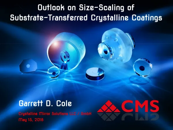
AlGaAs • Garret Cole (CMS) kindly created some slides regarding scaling AlGaAs.
Scalable Production Technique • Leverage semiconductor infrastructure for LIGO-scale optics • high-uniformity epitaxial growth on large-diameter substrates • void-free direct bonding of crystalline semiconductors • commercial tools available for LIGO-relevant mirror sizes
Scalable Production Technique Bonding: 45 cm GaAs wafers: 20 → 40 cm Epitaxy: 30 → 40 cm • Crystalline coatings limited to ⌀20 cm, three areas to scale • commercial GaAs wafers currently available up to 20-cm diam. • epitaxy qualified for wafer sizes of 30 cm (~50-cm chamber diam.) • semiconductor direct bonding demonstrated to diam. of 45 cm
LIGO-Scale GaAs Wafers • Promising discussions with Freiberger Compound Materials • currently produce GaAs wafers up to 20-cm diameter • VGF crystal growth capabilities up to ~40-cm max diameter • “waferizing” processes must be scaled up (main cost driver) • Estimated 2 year timeline and total cost of ~$5M
Step 2: LIGO-Scale Epitaxy • Ongoing discussions with external epi foundries (US based) • two options for production MBE reactors: • Veeco Gen2k or Riber7000/8000 • LIDAR and facial recognition is rapidly changing market • Estimated 3-4 year timeline and total cost of ~$7M-10M
Step 3: LIGO-Scale Bonding • Electronic Visions Group, key vendor for semicon. bonding • currently offer a production tool for 45-cm SOI manufacturing • SOI: silicon on insulator, wafers for microwave electronics • designed for 1-mm thick subs., must be modified for optics • Estimated 3-4(?) year timeline and total cost of ~$10M Si SiO2 Si
Penn/Harry/Cole: https://arxiv.org/pdf/1811.05976.pdf Fejer/Penn/Harry rechecking effect of thermoelastic contribution – these numbers are overly pessimistic! Steve Penn LIGO DCC - G1900684
AlGaP crystalline mirror technology Crystalline coatings – GaP growths underway
AlGaP crystalline mirror technology XRD Si Theory GaP measured GaP 300nm GaP coatings on Si
GaP and AlGaP/GaP loss: Cumming et al., Class. Quantum Grav. 32 (2015) 035002 Murray et al., Phys. Rev. D 95 (2017) 042004
MBE Others?!?! • AlGaN Growth on Al2O3, GaN or AlN. Issues of quality of films on Al2O3 cited by Novikov et al. Journal of Vacuum Science & Technology B 34, 02L102 (2016) AlGaP • Mechanical loss ︎✓ • Lattice matched to silicon ︎✓ • Not well-developed ✘ • Optical properties ✘ • Growing on 200kg scale optics ✘ AlGaAs • Developed technology ︎✓ • Optical performance ︎✓ • Grown on GaAs wafers ✘ • Requires transfer ✘ Common challenges: • electro-optic and piezoelectric effects (initial discussion Abernathy T1400726) • scaling (Cole estimated ~$40M for GaAs substrate + MBE + bonding tool) • Mechanical loss at RT on crystalline substrates • Scatter and absorption evaluation, effect of defect, large area • Who is doing the work? (how much will industry drive, how much do we need to do)? discussion...
