Download
1 / 9
110 likes | 257 Vues
<br>Get brief overview of manufacturing processes for semiconductor devices. To know more information please visit www.waferpro.com<br>

E N D
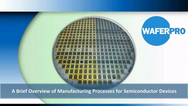
A Brief Overview of Manufacturing Processes for Semiconductor Devices
Television, radio, cell phone and other electrical or electronics goods have semiconductor devices in them. The materials used in semiconductor devices are capable of partially conducting electricity, unlike full conductors of electricity like aluminum, copper and steel. A semiconductor falls somewhere between a conductor and an insulator. For this reason they are commonly used to make Integrated Circuits. A good example of a semiconductor material is silicon. This is the most commonly used material in the microelectronics industry for various reasons. One of the primary reasons is its low price and availability.
An integrated circuit has various tiny components like resistors, diodes and transistors. These tiny components can damage easily if a large amount of current passes through them. So, a silicon wafer or substrate is usually used as a base rather than a conductor. This type of wafer also gives a better consistency for current flow compared to a conductor after special treatment. An integrated circuit is usually made up of a wafer, resistors and other electronic chips. This type of circuitry board plays a vital role for the functioning of electrical or electronics devices.
When it comes to the manufacturing of semiconductor devices, there are some key processes. Deposition, patterning, removal and modification of properties for electrical purposes are the main ones. Deposition refers to transferring or coating another material onto the substrate. This could be performed using technologies like physical vapor deposition or PVC and chemical vapor deposition or CVD.
In the case of removal process, dry or wet etching methods can be used to remove material from the semiconductor substrate. Patterning is shaping or reshaping of the substrate. One of the common methods is lithography. One of the most common methods for electrical property modification is ion implantation. As its name implies, ions are implanted onto the substrate to change its physical properties.
Wafer testing is carried out to test if it meets the required criteria. When it comes to making a thin layer of substrate as in the case of a PCMCIA or a smart card, grinding is performed to reduce the thickness. Other key processes are die preparation and IC packaging. Die preparation involves mounting chips onto a substrate and die cutting.
For IC packaging, some of the main processes are integrated circuit bonding and encapsulation. For integrated circuit bonding, wire or the rmosonic bonding can be used. Typical examples of IC encapsulation processes are plating and baking. Integrated circuit testing is critical to check the overall functions of microchips and substrate. It is the final testing of the whole device before packaging and shipment to a customer.
To summarize, semiconductor devices are used in all the current electrical or electronics products on the market. The manufacturing processes for these devices involves many steps. The major processes are wafer processing, die preparation and IC packaging. Integrated circuit testing is carried out to check the overall functions of all chips and substrate as final inspection before packaging and shipment to a customer.
Contact 410 E Santa Clara Street, #518, San Jose, CA 95113 Phone: (408) 622-9129 Email : sales@waferpro.com Fax : 4086229385 www.waferpro.com