Download
1 / 35
350 likes | 528 Vues
Photo and Dark Conductivity in Ordered Array of Nanocrystals. Andrew Shabaev * , Alexander L. Efros ** , and Alexei L. Efros ***. * George Mason University, ** Naval Research Laboratory, *** University of Utah. Supported : Office of Naval Research and Department of Energy.

E N D
Photo and Dark Conductivity in Ordered Array of Nanocrystals Andrew Shabaev*, Alexander L. Efros**, and Alexei L. Efros*** *George Mason University, ** Naval Research Laboratory, ***University of Utah Supported: Office of Naval Research and Department of Energy Submitted to Nano Letters
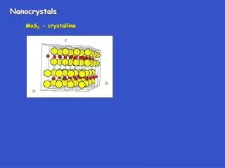
2a Egd ~5-7eV Egs ~2-3eV Nanocrystals are most heavily studied nano-scalesemiconductors ![A. Ekimov (1981) in semiconductor doped glasses and L. Brus (1983) in colloidal solutions, First theory of growth and optical properties :Al. L Efros and A. L. Efros (1982 ] Semiconductor Nanocrystals Nanocrystals: light TEM image of a bare CdSe nanocrystal Absorption band edge could be shifted up to ~1 eV
TOPO: TOP: P O=P Colloidal Semiconductor Quantum Dots (Nanocrystals): Cd Se CdSe nanocrystals Liquid-phase synthesis: • Crystallites of semiconductor • Coated with surfactants: • trioctylphosphine (TOP) • trioctylphosphine oxide (TOPO) 320 °C • diameters between 2 to 12 nm • size distributions <5% Murray, Norris, Bawendi; JACS 115, 8706 (1993). oleic acid: CdSe is the most heavily studied colloidal semiconductor nanocrystal
Size-Dependent Optical Properties Fluorescence CdSenanocrystals decreasingsize photo by Felice Frankel; samples by Bawendi Group (MIT) Tunable Fluorescence
et al. Nature Photonics 2013
Also Tunable Absorbance • Tune Color of Material With Size • Tailor absorption and fluorescence • Can use different semiconductors • Applications: • biological imaging • solid-state lighting • solar cells CdSe Murray, Norris, Bawendi; JACS 115, 8706 (1993).
Motivations 1. Electron mobility in nanocrystal solids has risen by more than five orders of magnitude to 27 cm2 /Vs Ji-HyukChoi et. al. Nano Lett. 2012, 12, 2631−2638 2. Photoconductivity in nanocrystalsolids exceeds dark conductivity by 2-4 orders of magnitude at relatively weak excitation generating much less than one electron-hole pair per nanocrystal. Jong-SooLee. et. al. Nature Nanotechnology, 2011, 6, 348 .
Low Mobility of “Localized States” vs High Mobility of “Nearly Free States” Photocurrent indicates a large change of the mobility stimulated by the light. where ndand dare the concentration and mobility of resident carriers, npand p are the concentration and mobility of carriers created by light. If p >> d significant increase of the current can be observed even at concentration of photoexcitedcarriers np<<nd. Nanocrystals embedded in glass matrix or polymer show well defined ionization threshold: e- fast nearly-free electrons slow transport of quasi-localized electrons U0=0.6-1.5 eV e-
Electrons in a Periodic Array of Nanocrystals Electron transport in quasi-ideal three dimensional periodic array of a radius nanocrystals, which has a cubic lattice with period b. Each NC is athree dimensional potential well for electrons, which has a form of the Woods-Saxon potential: where U0 is the depth of the potential, which is equal to the NC ionizations threshold, and parameter << ais due to a NC atomic structure, ~ (0.2-0.5)a0, where a0 is the lattice constant of a semiconductor. b b 2a 2a The periodic potential acting on electrons: where are the reciprocal vectors of a cubic lattice and
Nearly Free Electrons in a Periodic Array of Nanocrystals = k a U0 the origin of these parabolas is any reciprocal vector The electron dispersion changes near intersection points forming energy gaps: The band width Eof a Brillouinzone can be found using decreases with energy !!! The nearly-free electron approximation is applicable if the gaps are smaller than the band width. The ratio: 0.05 Near free approximation is valid.
Nearly Free Electron Transport Properties Scattering due to structural defects of the super-crystal:small fluctuations of the radii and positions of NCs. The transport time is e- scattering size and position fluctuations Scattering rate: where , and are the mean squared fluctuation of the NC radius and NC position displacement. For electrons created by Auger ionization processes, the energy is so high that τk ~ 1.2ps, and the length of flight during the relaxation time ~ 1m Calculating the photoconductivity and mobility of excited electrons requires the energy distribution function of hot electrons. Assuming majority of photoexcited carriers has photoexcitation energy, Ep~ 2eV, using
THE LOWEST ENERGY BAND AND DARK TRANSPORT = • where c=0.16, Ep=17.5 eV, Eg=1.84 eV, and =0.42 eV. • In CdSeNCs: First one should find the energy of the lowest level in a framework of the Kane model • where c=3.9, Ep=2.64 eV, and Eg=0.28 eV, = • In PbSe NCs:
Lowest Energy Band Basis Functions In the tight-binding approximation the basis functions are the wave functions of electrons in the ground state of single NCs: m* and m are the effective masses of an electron in the NC and the barrier, and E0 is the ground state energy of NC, which is determined by the smallest solution of the following equation: The normalization constant A is given by In small NC, nonparapolicity of the conduction band should be taken into account via energy dependence of the electron effective mass, m*(E).
Lowest Energy Band In the tight binding approximation the wavefunctions of the electron free motion can be represented as the Bloch sum In the limit the band energy spectrum is
WIDTH OF THE BAND In SC structure with 6 nns In CPH structure with 8 nns Note that THE MASS AT THE BOTTOM OF THE BAND IS
Dark Band Mobility The dark conductivity depends on the ratio of the band width to the temperature T At kBT< , transport within parabolic spectra, where The scattering transport time in parabolic spectra Using standard transport theory we obtain the mobility for nondegenerate electron gas where the maximum mobility is reached at b=2a For degenerate electron gas when EF >>kBT where τk is calculated with
Temperature Dependence of the Mobility at all Temperatures High temperature : temperature much larger than band width kBT >> Temperature enters into kinetic equations only through energy derivative of Boltzmann function: For all electrons in the band << kBT and the derivative is equal to Mobility: where with dimensionless variables
Dark Conductivity and Localization Localization occurs if a typical fluctuation of the energy of the NC ground state, E0, exceeds the band width, , by a some critical numerical factor Xc, when E0 >Xc . Most probable source of E0fluctuations is the fluctuations of the NCs radii a: in parabolic regime: For rectangular distribution of E0within the interval [- E0 /2, E0 /2] the critical broadening width, E0c was found to be E0c / = Xc 2.67. If random variable has rectangular distribution The critical broadening width
The Mott transition The band conductivity can be also suppressed by the Mott transition, that occurs even in the perfectly ordered system due to electron-electron interaction if the band is half filled. The transition is usually described in the framework of Hubbard's model. In the ordered array of NCs, the tight binding approximation should be modified by adding the energy of interactions of two electrons with the different spin orientation occupying the same NC (the Hubbard energy).The metal-insulator transition occurs in 2- and 3-dimensional cases if the Hubbard energy is larger then the band width The Hubbard interaction results in the energy gap between occupied and unoccupied states in the half field band, transforming metal into dielectric. The Hubbard gap can be observed in the optical absorption. If the Hubbard gap is smeared by disorder, the Anderson transition provides localization at all feeling factors inside the lowest band.
Correlation of dark conductivity and photoconductivity Without any disorder the overlapping ground states of the NCs form a band with a relatively high mobility. In this case the Auger processes are suppressed by the momentum conservation. In reality, even on the metallic side of the Anderson transition the metallic band may include a very small part of all NCs. The others form clusters of one ,two and more overlapping NC's that may provide the Auger ionization but does not participate in the dc conductivity. The number of such clusters gradually decreases with decreasing disorder. In a general case there are NCs that provide metallic type conductivity and there are NCs creating high energy electrons for the photoconductivity. As a result the increase of a dark conductivity should correlate with the decreasing production of photoelectrons.
Discussion of Experimental Results on Photoconductivity Auger-stimulated photocurrent could explain two orders of magnitude increase in current under optical excitation reported initially for array of In2 Se2-- capped CdSe/CdS core-shell NCs. 1. The increase of the carrier concentration in the ground conducting state is not sufficient for the explanation. 2. The similarity of spectral dependence of photo-current responsivityand absorption coefficient indicates that each photon absorbed by charged NCs transfers the resident electron into highly conductive state. Jong-SooLee. et. al. Nature Nanotechnology, 2011, 6, 348 3. These states are quasi-free electrons whose mobility is at least two orders of magnitude higher than the mobility of electrons in ground states.
Discussion of Experimental Results on Photoconductivity Existence of highly mobile quasi-free carriers created by photons is convincingly demonstrated by experiments conducted in PbS NC solid. P. Nagpal and V. I. Klimov, Nature Communications 2, 486 (2011) 1. Burst of photoconductivity at U00.9eV connected with photo-excitation of resident holes above the NC ionization threshold 2. Burst of photoconductivity at 1.5 eVcan be explained by Auger auto-ionization of charged NCs . 3. Addition broad bump in the photocurrent near Eg +U0 2.2 eVcan be explained by direct NC ionization. 4. The additional feature at 3.3 eVcan be explained by excitation above the localization threshold of the NC solid at Eg+2U03.1 eV.
Discussion of Experimental Results on Dark Conductivity The largest dark mobility of27 cm2 /(Vs) was reported in the array of closely packed CdSeNC with 2a= 3.9nm. Such mobility indeed could be reached in ordered array of NCs with NC size dispersion =5% and confinement potential U0< 1eV. Ji-HyukChoi et. al. Nano Lett. 2012, 12, 2631−2638
Summary • We developed a theory of the photo- and dark conductivity in ordered arrays of NCs. Electron transport properties were calculated for scattering by structural defects of super-crystal, namely small fluctuations of the radii and positions of NCs. • For dark conductivity, we found the the diagram in axis a and b separating Anderson localized states with the hopping conductivity and band states with the metallic type conductivity. The possibility of the Mott transition is also considered • We propose a new mechanism of photoconductivity triggered by very efficient Auger recombination of electron-hole pairs at the band edge of NCs, which transfers electrons localized in the NCs into high energy quasi-free states of the NC array. This leads to the 2 - 4 orders of magnitude increase of the photo-current because the mobility of these states is 4 - 5 orders of magnitude larger than the mobility of electrons in the ground state. • Our theory predicts a correlation between dark and photo conductivitiy.
Four Mechanisms of Nearly Free State Photo-activations Each mechanism requires a different photon energy. Photons with energy above the NC band gap create quasi-free electrons via so called Auger auto ionization of charged NC. Possible only if the NC contains at least one resident electron. Auger photoexcitation mechanism is unique property of NCs because the rate of Auger processes in NCs is much larger than the rate of the radiative recombination. As a result quasi-free carriers are generated with almost 100% probability.