Download
1 / 24
260 likes | 541 Vues
Radiation hard Si detectors. Eduard Monakhov University of Oslo. RD50 Collaboration Radiation hard semiconductor devices for very high luminosity colliders. (http://rd50.web.cern.ch/rd50/). Physical Electronics group Centre for Materials Science and Nanotechnology University of Oslo.

E N D
Radiation hard Si detectors Eduard Monakhov University of Oslo RD50 Collaboration Radiation hard semiconductor devices for very high luminosity colliders. (http://rd50.web.cern.ch/rd50/)
Physical Electronics group Centre for Materials Science and Nanotechnology University of Oslo ...inside MiNa-lab
Outline • Motivations: the LHC upgrade • The RD50 Collaboration • Radiation effects in silicon detector • Improving Si radiation hardness • Thin detectors: thinned and epitaxial • 3-D and Semi 3-D detectors • Summary
Motivations: the LHC upgrade Radial distances Expected S-LHC of the actual tracker fluence for fast hadrons 4 cm 1.6x1016 cm-2 11 cm 2.3x1015 cm-2 22 cm 8x1014 cm-2 115 cm 1x1014 cm-2 The current detector technologies can operate up to ~1015 cm-2
The RD50 Collaboration RD50: Development of Radiation Hard Semiconductor Devices for High Luminosity Colliders 1. Formed in November 2001 2. Approved by CERN in June 2002 • Main objective: • Development of ultra-radiation hard semiconductor detectors for the luminosity upgrade of LHC to 1035 cm-2s-1 (S-LHC) • Challenges: • - Radiation hardness up to fluences of 1016 cm-2 required; • - Fast signal collection (10 ns); • - Cost effectiveness. Presently 280 Members from 55 Institutes Belgium (Louvain), Canada (Montreal), Czech Republic (Prague (2x)), Finland (Helsinki (2x), Oulu), Germany (Berlin, Dortmund, Erfurt, Halle, Hamburg, Karlsruhe), Greece (Athens), Israel (Tel Aviv), Italy (Bari, Bologna, Florence, Milano, Modena, Padova, Perugia, Pisa, Trento, Trieste, Turin), Lithuania (Vilnius), Norway (Oslo (2x)), Poland (Warsaw), Romania (Bucharest (2x)), Russia (Moscow (2x), St.Petersburg), Slovenia (Ljubljana), Spain (Barcelona, Valencia), Sweden (Lund) Switzerland (CERN, PSI), Ukraine (Kiev), United Kingdom (Exeter, Glasgow, Lancaster, Liverpool, London, Sheffield, University of Surrey), USA (Fermilab, Purdue University, Rutgers University, Syracuse University, BNL, University of New Mexico)
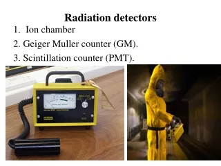
Radiation effects in silicon detector Silicon particle detectors 0 V, pre-amp. • Advantages: • high signal-to-noise ratio • fast direct charge readout • high spatial resolution p+ e h n- e h e h n+ Ubias - p+ - - + + n+ +
Radiation effects in silicon detector Damage of the crystal lattice Electronic levels of main electron traps in Si: V VO V2 Ec -/0 =/- Ec-0.23 eV Ec-0.18 eV Cs I -/0 Ec-0.44 eV 0/+ Ev+0.20 eV Oi Ev
Radiation effects in silicon detector I. Increase of the leakage current The leakage current density (J)linearly increases with the particle fluence (F): J= • Increase of power dissipation: P=VxI • Increase of voltage drop on bias resistors: V=RxI • Decrease of the S/N ratio
Radiation effects in silicon detector II. Effect on doping • If Vdep is too high, the detector cannot operate fully depleted • Decrease of the charge collection efficiency • Decrease of the S/N ratio
Radiation effects in silicon detector III. Charge trapping & recombination - p+ - - + + + n+ • Increase of charge collection time • Decrease of the charge collection efficiency • Decrease of the S/N ratio
Improving Si radiation hardness Defect engineering VO V2 Ec -/0 =/- Ec-0.23 eV Ec-0.18 eV -/0 Ec-0.44 eV 0/+ Ev+0.20 eV Ev V + O VO V + V V2 Leakage current as a function of the bias in silicon detector with different types of defects (SILVACO TCAD).
Improving Si radiation hardness Defect engineering: The effect of C and O on radiation hardness standart FZ-Si: [O]~1016 cm-3 oxygenated FZ-Si: [O]~1-4x1017 cm-3
Improving Si radiation hardness The neutron puzzle No radiation hardening for neutron radiation!
Improving Si radiation hardness Magnetic Czochralski (MCZ) silicon standart FZ-Si: [O]~1016 cm-3 oxygenated FZ-Si: [O]~1-4x1017 cm-3 MCZ-Si: [O]~1018 cm-3 Higher radiation tolerance... ...but the same 'neutron problem'.
Improving Si radiation hardness Summary Ways to improve radiation hardness of Si: • Oxygenation (shallow VO instead of deep levels) • Decrease in carbon content (C effects vacancy-interstitial annihilation) • Hydrogenation (H passivates dangling Si bonds) • Creation of electrically inactive extended defects (sink for vacancies and interstitials)
Thin detectors Advantages: 1. Smaller leakage current: IleakW 2. Smaller depletion voltage: Vdep=qW2Neff/2W2 3. Lower probability for trapping and recombination (W) Disadvantage: Smaller amount of carriers generated by a particle, i.e., smaller amplitude of the signal (W)
Thin detectors FZ thinned devices (W=50 mm) SEM: back view of a thinned device Area: 1 mm2 - 20 mm2 and I<1 nA/cm2 at 20 V Front (left) and back (right) view of thinned devices Area: 10 mm2 and I<1 nA/cm2 at 20 V
Thin detectors FZ thinned devices (W=50 mm): Radiation hardness 20 GeV proton irradiation: p=9.5x10¹³-8.6x1015 cm-2 for W=300 µm at =8.6x1015 cm-2: Vdep~2300 V
Thin detectors Epitaxially grown layer (W=50 µm) p+ n n+ The smaller thickness of the detecting region (epi-layer) allows to increase the doping and still use relatively low bias ( Wsqrt{V/Nd} ) Higher doping shifts the SCSI point to higher fluences.
3D detectors • Proposed by S.I. Parker, C.J. Kenney and J. Segal (NIM A 395 (1997) 328) • Called 3-D because, in contrast to silicon planar technology, have three dimensional (3-D) electrodes penetrating the silicon substrate • Important researches are now under investigation by a collaboration (not in RD50) within Brunel Univ., Hawaii Univ., Stanford Univ. and CERN Conventional (a) and 3D (b) detectors: a) b) depletion thickness depends on p+ and n+ electrode distance, not on the substrate thickness (1) can operate at very low voltages or (2) can have a high doping for ultra-high radiation hardness
3D detectors Charge collection in 3D detectors • lower collection length than planar technology • lower charge collection time than planar technology • higher charge collection efficiency computer simulations of the charge collection dynamics for planar and 3D detectors
3D detectors Real devices a 3D detector structure: a 3D structure grown at SINTEF: 15 m 200 m 4 m
Semi-3D detectors Proposed by Z. Li(NIM A 478 (2002) 303). Single-side detectors with alternative p- and n- strips on the front side After SCSI, the depletion occurs from both sides reducing the needed depletion voltage by factor 2.5
SUMMARY • There is considerable activity and progress in improving radiation hardness of Si particle detectors • On the 'material side', using the so-called defect engineering, the range of working fluences has been extended to above 1015 cm-2(not to mention pure scientific results within the physics of semiconductors) • The progress in semiconductor microtechnology allows to design detector structures with 'inherited' ultra-high radiation tolerance