Download
1 / 19
190 likes | 305 Vues
This experiment focuses on function reduction theories and practical implementations in the CPE 169 Digital Design Laboratory. It explores techniques to minimize digital circuit implementations, emphasizing cost-effectiveness through Boolean algebra and Karnaugh Maps. The procedure involves downloading circuit files, creating truth tables, applying function forms, and using VHDL for FPGA implementation. Students will compare results, finalize reports, and ensure instructor approval, enhancing their understanding of digital design methodologies.

E N D
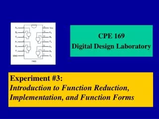
Experiment #3A:Introduction to Function Reduction, Function Forms, and VHDL Implementation CPE 169 Digital Design Laboratory
Function Reduction • General approach: make function smaller • Underlying purpose: make it cheaperto implement the function. • True definition dependent upon how “cheaper” is defined • General correlation between a “reduced function” and an inexpensive implementation
Minimum Cost Implementation • Based on definition of “cost” • Cost has no absolute definition: • Could include: • Cost of components (digital IC’s, circuit board,…) • Cost of development (engineering labor, tools,…) • Cost of manufacturing (tooling, test fixtures,…) • Component Costs change with: • current part availability and/or pricing • quantity discounts • changes in technology • Our metrics: • # of IC’s • # of Gates (including NOT gates) • # of Gate Inputs • # of Literals • Experiment 3: minimum cost defined by the number of gates required to implement function.
Reducing Functions • Computer-based methods • fast, concise but cookbook approach • Boolean algebra • instructive but slow, error prone • Karnaugh Maps • fun and exciting but limited to functions of 4 - 5 variables
Function Forms • Boolean functions can be used to describe complex operations such as adders, multipliers, etc. • Infinite number of different circuits can be used to implement any given function • Standard function forms: • SOP (AND/OR) • POS (OR/AND) • Several common forms are derived from SOP and POS using DeMorgan’s theorem
DeMorgan’s Theorems • Can be used to generate different function forms:
Experiment 3a Procedure Overview • Download circuit from CPE 169 website • .bit file (Nexys) • Analyze the implemented function • Create a Truth Table (include in report!!) • Reduce the function to minimized SOP & POS forms • K-Maps (include in report!!) • Implement the function on the Nexys and breadboard using discrete logic IC’s: (Don’t forget detailed schematics in report!!) • NAND / NAND form (SOP) • NOR / NOR form (POS) • Implement the function on the Nexys FPGA using VHDL • Using VHDL and the Xilinx Tools • Compare all results • Get Instructor Sign-off Sheet & signature (include in report!)
Xilinx Design Methodology • The steps required in order to model, simulate and implement a circuit using the Xilinx ISE software • Basic steps are as simple or as complicated as you want to make them • Xilinx ISE and VHDL used again in CPE 229/269/329 and CSC 315
Basic Xilinx Design Flow 1) VHDL source code generates a description of circuit. 2) VHDL source is translated into intermediate form for use by other software used in the design flow. 3) Test Bench Waveform software generates signals to verify circuit operation using the ModelSim XE simulator. 4) Circuit inputs and outputs are “mapped” to FPGA pins externally hardwired to I/O devices on the Nexys board. 5) The circuit design is downloaded into the FPGA. (Use Digilent ExPORT for Nexys USB port) 6) Proper operation of the circuit is verified.
Add your logic expression to the VHDL code module template Your definition of input / output signals is turned into a VHDL “Entity” Insert code here
Circuit Connections to Development Board FPGA J14 J15 K15 K14 H18 K18 K17 L14 A B C D LDO LD1 LD2 LD3 F1 F2 SW1 SW2 SW3 SW4 Nexys-2 Board • Assign Package Pins • Maps Input/Output Circuit Signals to FPGA Pins • Puts Info in a “Constraints” File
A Little “Sage Advice” • Since this is your first time using the tools, be sure to follow allof the steps, in the order given. • Skipping steps may result inhorrendouslyhideousoutcomes that you really don’t want to experience. • A confused CAD tool is not a happy CAD tool!;( • Be sure to read the Explanations as you proceed, so that you begin to understand whyyou are doing what you are doing.
Note for Next Week BEFORE LAB: • Be sure to run through the B2 Spice A/D Tutorial (on the CPE-169 website) Brief overview of the logic circuit simulation tool you will be using in next week’s lab