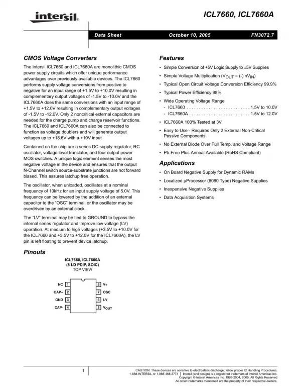
Monolithic sensors in high-voltage deep-submicron technology
1.15k likes | 1.52k Vues
Monolithic sensors in high-voltage deep-submicron technology. Ivan Peric University of Heidelberg, Germany. Introduction to pixel sensors in high voltage CMOS technology Operation principle, advantages and disadvantages Summary of the project results Pixel types

Monolithic sensors in high-voltage deep-submicron technology
E N D
Presentation Transcript
Monolithic sensors in high-voltage deep-submicron technology Ivan Peric University of Heidelberg, Germany
Introduction to pixel sensors in high voltage CMOS technology • Operation principle, advantages and disadvantages • Summary of the project results • Pixel types • 1) Particle sensitive pixels with complex CMOS electronics • Test chip in 180nm technology • 2) Integrating pixels with simple “4T” electronics • 4PMOST source follower pixels • 4PMOST pixels with voltage amplification • >4T CDS pixels • Test beam and lab measurements
Pixel detector in HV CMOS technology • Monolithic pixel sensor • 100% fill-factor • In-pixel CMOS signal processing • Good timing properties (theoretically 40 ps signal collection time) • Radiation hard (tested to 50 MRad (x-rays) and 1015 neq (protons)) • Not expensive (monolithic sensor, no bumping, standard technology used) • 350nm technology: 8 inch wafer run: 90k€ (350nm) • 180nm technology: 120k€ and 1.5k€/wafer (1 wafer ~ 200 cm2) • Allows thinning
Detector structure • The sensor is based on the “deep” n-well in a p-substrate • Main properties: • 1) Charge collection is based on drift • 2) CMOS signal processing electronics
Detector structure Pixel electronics in the deep n-well P-substrate Deep n-well NMOS transistor in its p-well PMOS transistor The CMOS signal processing electronics are placed inside the deep-n-well.PMOS are placed directly inside n-well, NMOS transistors are situated in their p-wells that are embedded in the n-well as well.
“Smart” diode array - SDA Pixel electronics in the deep n-well P-substrate Deep n-well NMOS transistor in its p-well PMOS transistor Smart diode
SDA in high voltage CMOS technology Pixel electronics in the deep n-well P-substrate Deep n-well NMOS transistor in its p-well PMOS transistor E-field Particle
SDA in high voltage CMOS technology • Although this structure can be implemented in any CMOS technology (see 65nm pixel), the best results are achieved when a standard high voltage CMOS technology with twin well is used. • A lowly-doped deep n-well can be then used. Such an n-well can be reversely biased with a high voltage. • In the process we used, we expect a depleted area thickness of 14 μm (20cm substrate resistance -> acceptor density ~ 1015 cm-3) • We measure a MIP signal of ~ 2000e, ~ 50% probably originates from undepleted bulk. • The charge generated by ionizing particles in the depleted area is collected by drift. Due to high electric field and small drift path, charge collection is very fast. We estimate ~ 40ps. • Due to drift based charge collection we have high radiation tolerance
Strong points • 1) Monolithic sensor • 2) CMOS in-pixel electronics • 3) Fast signal collection • Theoretically 40ps • 4) Thinning possible • Since the charge collection is limited to the chip surface, the sensors can be thinned • 5) Price and technology availability • Standard technology without any adjustment is used • Many industry relevant applications of HV CMOS technologies assure their long tern availability • 350nm technology: 8 inch wafer run: 90k€ (350nm) • 180nm technology: 120k€ and 1.5k€/wafer (1 wafer ~ 200 cm2) • 6) High tolerance to non-ionizing radiation damage • High drift speed • Short drift path • 7) High tolerance to ionizing radiation • Deep submicron technology • Radiation tolerant design can be used • PMOS transistors, that are more tolerant to radiation, can be used (in contrast to MAPS with high-resistance substrate)
Drawbacks • 1) Capacitive feedback • We can implement the majority of important pixel circuits in CMOS, like the charge sensitive amplifier, shaper, tune DAC, SRAM but… • “Digitally active” CMOS logic gates in pixels should be avoided • Possibility 1: Current mode logic can be used instead CMOS (drawback – current consumption ~ 1 A / digital gate) • Possibility 2: Separate digital and analog circuits (drawback – a few per cent of inactive area at the chip edge) • 2) Relatively large size of the collecting electrode • Typical values for the total n-well capacitance are • 10fF - small 21x21 m2 pixels and simple pixel electronics (already tested) • 200fF 55x55 m2 CMOS pixels (already tested) • 700fF 80x400 m2 CMOS pixels (proposed long pixels for SLHC) • 3) Lower signals than in the case of fully depleted sensors • The signals do not decrease significantly after irradiation to 1015 neq cm2
Results of the Project • The SDAs have been developed within a small project whose aim was the proof of principle • CMOS particle sensitive (“intelligent”) pixels in 350nm technology • In pixel hit-detection and binary trigger based readout (similar to ATLAS pixels). Pixel size is 55x55m2 • Noise of 60e • Direct hit signal - 1800e, leading to a seed pixel SNR of 30 • Signal delay time ~ time resolution of the detector ~ 120ns • Part of the signal originates from the un-depleted bulk and is collected by diffusion – impact on timing will be investigated on a test chip, probably not an issue • 4-transistor pixels (PM Chip) in 350nm technology • Test beam: • Efficiency 97.5% • MIP cluster signal is 2000e and seed pixel signal 1200e • The noise is about 44e that is twice as large as in lab tests – non-ideal setup • Seed pixel SNR is 27, Cluster Signal/Seed Noise = 47 • We measure spatial resolution < 3.8μm
„Intelligent“ particle sensitive pixel in 350nm technology Preamplifier (NMOS part) Preamplifier (NMOS part) RC-CR shaper 4-bit SRAM NMOS based comparator 4-bit threshold DAC 55m CM NMOS logic
„Intelligent“ particle sensitive pixel in 350nm technology Preamplifier (NMOS part) Preamplifier (NMOS part) RC-CR shaper 4-bit SRAM NMOS based comparator 4-bit threshold DAC 55m CM NMOS logic
4T pixel in 65nm technology Metal-metal coupling capacitor 2.5m Here only the standard N-Well has been used, only PMOS electronics Lower signals expected (small depleted volume) We hope to compensate this by lower detector capacitance
Radiation tolerance • In order to test the radiation tolerance we have performed a few irradiations
Proton irradiation • Proton irradiation of continuous readout pixels up to 1015 neq/cm2, which corresponds to a dose of ~300MRad in SiO2. • As expected, we measure an increased noise. For example, at 20C we measure 270e. (We had 12e before irradiation.) However, only a light cooling leads to significant noise improvement, a sign that the noise is caused by leakage current. At 10C we have a noise of 77e and at -10 only 40e. • We have measured the response to 22Na beta particles. SNR at -10C is 93.
Irradiation with protons (1015 neq/cm2, 300 MRad) 55Fe spectrum, RMS noise Irradiated 10C RMS Noise 77 e 55Fe spectrum and RMS noise Not irradiated Room temperature RMS Noise 12 e
Irradiation with protons (1015 neq/cm2, 300 MRad) SNR = 93 -10C
Particle sensitive pixels with CMOS electronics and continuous readout
3.3 V CR-RC Comparator CSA AC coupling -50 V N-well P-substrate Signal detection
Signal detection 3.3 V CR-RC Comparator CSA AC coupling -50 V N-well P-substrate
Signal detection 3.3 V CR-RC Comparator CSA AC coupling -50 V N-well P-substrate
Signal detection 3.3 V CR-RC Comparator CSA AC coupling -50 V N-well P-substrate
Signal detection 3.3 V CR-RC Comparator CSA AC coupling -50 V N-well P-substrate
Signal detection 3.3 V CR-RC Comparator CSA AC coupling -50 V N-well P-substrate
Signal detection 3.3 V CR-RC Comparator CSA AC coupling -50 V N-well P-substrate
Signal detection 3.3 V CR-RC Comparator CSA AC coupling -50 V N-well P-substrate
Intelligent particle sensitive pixels – possible application • Vertex detector for the novel experiment. Goal: search for lepton flavor violating decay -> eee • Four layers of pixels ~ 80x80m2 size • Continuous muon beam stopped at target – 109 muon stops/s –> requires time stamping with ~ 100ns resolution • Energy range of interest: 15-50MeV –> multiple scattering dominates momentum measurement –> ~50 m thin detector
Multi-reticle module Module Chip2 Chip2 Pads Chip to chip connections Chip1 Chip1 Reticle1 Reticle2 Chip to reticle edge distance = 80 um 2.0 cm Pixel modules with (almost) no insensitive area can be produced Reticle-reticle connections can be made easily by wire bonding Instead of wire-bonding, an extra metal layer can be used as well
Low-mass detector Module (length. 12 cm, width 1cm, the figure is not scaled) chip to chip connections Pads for power and IO signals Chip (reticle 2) Chip (reticle 3) Carrier Large sensitive area without material Interaction region Wire as support Very low-mass only silicon module
Analog Pixel Bias Volt. Comparator To digital channel CSA Threshold DAC SRAM N-well P-substrate
Digital Channel From Analog Pixel Priority In LE RAM S Hit R Addr ROM Priority Out Read Time Stamp Data Bus
Detector with separated analog and digital pixels 250 pixel rows (80 μm pitch) 2cm Reticle1 Analog Pixels – Sensitive Area 1cm ~125 pixel rows (80 μm pitch) ~0.75mm Digital Channels Analog Pixels The figure shows one reticle LVDS Out ~0.7m Digital Channels
Test Chip in 180nm technology 39m 1.8mm 42x36 pixels 30m Analog pixels 0.7m 2 metal layers Analog pixel layout Digital channels Pixel is made smaller than needed This has positive impact on detector capacitance
Analog Pixel Bias Volt. Buffer To digital channel CSA N-well P-substrate The analog pixel is slightly different than required for the final design Comparator, tune DAC and SRAM are missing (placed in the digital channel)
Digital Channel with tune DAC HitEn Base line Comparator In Global thr. Trigger In ROEn Latch Threshold DAC Reset Hit bus Data out The digital channel is slightly different than required for the final design Similar number of transistors
Digital Channel with e-fuse This NMOS takes care that the other transistors do not see the high voltage required for “burning” the fuse E-fuse 3.6V or global thr. 1.8V HitEn Base line Comparator In „1“ In y ROEn x Reset E-fuse substitutes threshold tune DAC -> smaller layout Idea: Strasbourg “MAPS” group (A. Dorokhov) E-fuse requires high voltage to be “burned”
Digital Channels Fuse Fuse-“addressing“ transistors DAC 39m 12m Latches
Time walk - simulation 6000e 1200e 6 sigma noise 7ns!!! Power in analog pixel ~ only 8W
Integrating pixels with source follower readout 3.3V Out 2V Res Res Sel Source follower Sensor diode -60V Only PMOS transistors -> no need for P-Well
Integrating pixels with source follower readout 3.3V Out 2V Res Res Sel -60V Reset phase
Integrating pixels with source follower readout Out Sel -60V Signal detection phase
Integrating pixels with source follower readout Out Sel Q/Cdet Q Cdet -60V Signal detection phase
Integrating pixels with source follower readout Leakage current -> noise, pedestal dispersion 3.3V Out 2V Res Res Sel Threshold dispersion -> pedestal dispersion Source follower -60V The main problems: KTC noise -> requires CDS Leakage current (leakage of PMOS switches probably dominates) Leakage current causes noise and pedestal dispersion Threshold dispersion
Integrating pixels with voltage amplification VP VP Res Res Sel Out
Integrating pixels with voltage amplification VP VP Res Res Sel Out Reset phase
Integrating pixels with voltage amplification VP Charge sensitive amplifier Sel Out Signal detection phase
Integrating pixels with voltage amplification VP Q/Cf Cf Sel Out Q Signal detection phase
Integrating pixels with voltage amplification VP VP Res Leakage current -> noise, pedestal dispersion Gets worse with higher reverse bias Probably a kind of back gate effect More pronounced than in source follower pixels Res Sel Out The main problems: KTC noise -> requires CDS PMOS leakage current Threshold dispersion is not the issue since its effect is reduced by applied gain