Insights from Clemson Summer School 2007: Advancing Photovoltaic Technologies
930 likes | 1.06k Vues
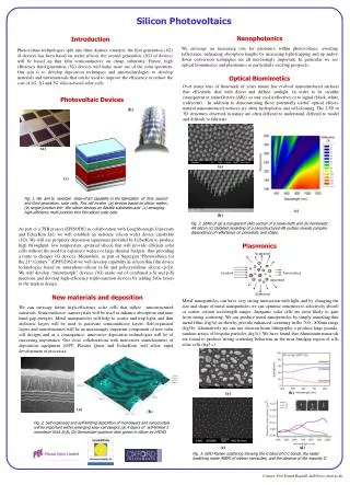
The Clemson Summer School 2007, led by Dr. Karl Molter from FH Trier, explored the latest advancements in photovoltaic (PV) technologies and their applications. Participants gained a comprehensive understanding of solar cell physics, technologies, and system components, highlighting the significant role of photovoltaics in solar energy conversion. The curriculum covered topics such as the photoelectric effect, solar cell characteristics, and integration of PV into buildings. With the growing importance of solar energy, this program aimed to educate and inspire future leaders in the field.

Insights from Clemson Summer School 2007: Advancing Photovoltaic Technologies
E N D
Presentation Transcript
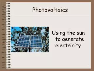
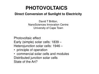
Photovoltaics Clemson Summer School 4.6. – 6.6.2007 Dr. Karl Molter FH Trier www.fh-trier.de/~molter molter@fh-trier.de Technology Components and Systems Applications
Content • Solar Cell Physics • Solar Cell Technologies • PV Systems and Components • PV Integration into buildings Clemson Summer School 2007 Dr. Karl Molter / FH Trier / molter@fh-trier.de
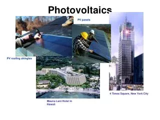
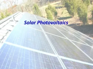
Introduction Photovoltaics, or PV for short, is a solar power technology that uses solar cells or solar photovoltaic arrays to convert light from the sun into electricity. Photovoltaics is also the field of study relating to this technology and there are many research institutes devoted to work on photovoltaics. The manufacture of photovoltaic cells has expanded in recent years, and major photovoltaic companies include BP Solar, Mitsubishi Electric, Sanyo, SolarWorld, Sharp Solar, and Suntech. Total nominal 'peak power' of installed solar PV arrays was around 5,300 MW as of the end of 2005 and most of this consisted of grid-connected applications. Such installations may be ground-mounted (and sometimes integrated with farming and grazing) or building integrated. Financial incentives, such as preferential feed-in tariffs for solar-generated electricity, have supported solar PV installations in many countries including Germany, Japan, and the United States. Clemson Summer School 2007 Dr. Karl Molter / FH Trier / molter@fh-trier.de
1. Solar Cell Physics • Solar Cell and Photoelectric Effect • The p/n-Junction • Solar Cell Characteristics Clemson Summer School 2007 Dr. Karl Molter / FH Trier / molter@fh-trier.de
History • 1839: Discovery of the photoelectric effect by Bequerel • 1873: Discovery of the photoelectric effect of Selen (change of electrical resistance) • 1954: First Silicon Solar Cell as a result of the upcoming semiconductor technology ( = 5 %) Clemson Summer School 2007 Dr. Karl Molter / FH Trier / molter@fh-trier.de
h • Light absorption • Generation of „free“ charges + • effective separation of the charges - Solar Cell and Photoelectric Effect Result: wearless generation of electrical Power by light absorption Clemson Summer School 2007 Dr. Karl Molter / FH Trier / molter@fh-trier.de
• • • • • • • • energy-states in solids:Band-Pattern Atom Molecule/Solid energy-states Clemson Summer School 2007 Dr. Karl Molter / FH Trier / molter@fh-trier.de
energy-states in solids:Insulator electron-energy conduction-band bandgap EG (> 5 eV) Fermi- level EF valence-band Clemson Summer School 2007 Dr. Karl Molter / FH Trier / molter@fh-trier.de
Terms: Fermilevel EF: limit between occupied and non occupied energy-states at T = 0 K (absolute zero) valence-band: completely occupied energy-band just be- low the Ferminiveau at T = 0 K, the electrons are „fixed“ (tightly bound) inside the atomic structure conduction-band: energy-band just above the valence-band, the electrons can move „freely“ bandgap EG:distance between valance-band and conduction band Clemson Summer School 2007 Dr. Karl Molter / FH Trier / molter@fh-trier.de
energy-states in solids :metal / conductor electron-energy Fermi- level EF conduction-band Clemson Summer School 2007 Dr. Karl Molter / FH Trier / molter@fh-trier.de
energy-states in solids:semiconductor electron-energy conduction-band bandgap EG ( 0,5 – 2 eV) Fermi- level EF valence-band Clemson Summer School 2007 Dr. Karl Molter / FH Trier / molter@fh-trier.de
Electron-Energy At T=0 (absolute zero of temperature) the electrons occupy the lowest possible energy-states. They can now gain energy in two ways: • Thermal Energy: kT (k = Boltzmanns Constant, 1.381x10⁻²³ J/K, T = absolute temperature in Kelvin) • Light quantum absorption: h (h = Plancks Constant, h = 6.626x10⁻³⁴ Js, = frequency of the light quantum in s-1). If the energy absorbed by the electron exceeds that of the bandgap, they can leave the valence-band and enter the conduction-band: Clemson Summer School 2007 Dr. Karl Molter / FH Trier / molter@fh-trier.de
x h h x Generation Recombination + + - - energy-states in solids:energy absorption and emission electron-energy conduction-band EF valence-band Clemson Summer School 2007 Dr. Karl Molter / FH Trier / molter@fh-trier.de
energy-states in semiconductorsphysical properties: thermal viewpoint: The larger the bandgap the lower is the conductivity. Increasing temperature reduces the electrical resistance (NTC, negative temperature coefficient resistor) optical viewpoint: the larger the bandgap the lower is the absorption of light quantums. Increasing light irradiation decreases the electrical resistance (Photoresistor) Clemson Summer School 2007 Dr. Karl Molter / FH Trier / molter@fh-trier.de
IIIB IVB VB Si B P 14 5 15 doping of semiconductors In order to avoid recombination of photo-induced charges and to „extract“ their energy to an electric-device we need a kind of internal barrier. This can be achieved by doping of semiconductors: „Doping“ means in this case the replacement of original atoms of the semiconductor-material (e.g. Si) by different ones (with slightly different electron configuration). Semiconductors like Silicon have four covalent electrons, doping is done e.g. with Boron or Phosphorus: Clemson Summer School 2007 Dr. Karl Molter / FH Trier / molter@fh-trier.de
energy-band view conduction-band majority carriers P+ P+ P+ P+ P+ P+ EF Si Si Si Si Si Si Si Si Si donator level valence-band - - - - - - - N - Doping crystal view n-conducting Silicon Clemson Summer School 2007 Dr. Karl Molter / FH Trier / molter@fh-trier.de
energy-band view conduction band B- Si Si Si Si Si Si Si Si Si EF acceptor level B- B- B- B- B- majority carriers + + + + + + + valence-band P - Doping crystal p-conducting Silicon Clemson Summer School 2007 Dr. Karl Molter / FH Trier / molter@fh-trier.de
depletion-zone Diffusion Ud EF P+ P+ P+ P+ P+ B- B- B- B- B- + + + + + + Diffusion p – type region Ed - + n – type region internal electrical field - - - - - - p/n-junction without light Band pattern view Clemson Summer School 2007 Dr. Karl Molter / FH Trier / molter@fh-trier.de
E = h photocurrent + + + + + + - irradiated p/n-junction band pattern view (absorption p-zone) depletion-zone - - - - - Ud EF P+ P+ P+ P+ P+ B- B- B- B- B- Ed p–type region - + n–type region Internal electrical field Clemson Summer School 2007 Dr. Karl Molter / FH Trier / molter@fh-trier.de
- - - - - - - - - - - - - - - - - - - - - - - - + + + + + + + + + + + + + + + + + + + + + + + + p-silicon + + + + + + + + + + + + + + + + + + + + + + + + + + + + + + + + + + + + + - + + + + + + + + + + + + + + - - - - - - - - - - - - diffusion E electrical field + + + + + + + + + + + + + - - - - - - - - - - - - - - - n-silicon - - - - - - - - - - - - depletion zone - - - - - - - - - - - - - - - - - - - - - - - - p/n–junction without irradiation(semiconductor diode)crystal view Clemson Summer School 2007 Dr. Karl Molter / FH Trier / molter@fh-trier.de
h + + + + + + + + + + + + + p-silicon + + + + + + + + + + + + + + + + + + + + + + + + + + + + + + + + + + + + + + + + - - - - - - - - - - - - diffusion E electrical field + + + + + + + + + + + + - - - - - - - - - - - - - - - - - - n-silicon - - - - - - - - - - - - depletion zone - - - - - - - - - - - - drift - - - - - - - - - - - - - p/n–junction with irradiationcrystal view Clemson Summer School 2007 Dr. Karl Molter / FH Trier / molter@fh-trier.de
Charge carrier separation within p/n–junction diffusion: from zones of high carrier concentration to zones of low carrier concentration (following a gradient of electrochemical potential) drift: driven by an electrostatic field established across the device Clemson Summer School 2007 Dr. Karl Molter / FH Trier / molter@fh-trier.de
Front-contact - hn Antireflection- coating n-region p-region ~0,2µm + + + + + + + + + + + - - - - - - - - - - ~300µm depletion zone Backside contact The real Silicon Solar-cell Clemson Summer School 2007 Dr. Karl Molter / FH Trier / molter@fh-trier.de
ISG IL IPH RS ID current source RP RL USG UL UD Equivalent circuit of a solar cell IPH: photocurrent of the solar-cell ID /UD: current and voltage of the internal p-n diode RP: shunt resistor due to inhomogeneityof the surface and loss-current at the solar-cell edges RS: serial resistor due to resistance of the silicon-bulk and contact material ISG/USG: Solar-cell current and voltage RL/IL/UL: Load-Resistance, current and voltage ISG = IL, USG = UL Clemson Summer School 2007 Dr. Karl Molter / FH Trier / molter@fh-trier.de
ID diode- characteristic ID ISG UD=USG UD RL RL= RL=0 MPP ISG / PSG Load resistance ISG = I0 = IK solar-cell characteristics ID IMPP Power MPP = Maximum Power Point USG UMPP U0 Solar-Cell characteristics simplified circuit Clemson Summer School 2007 Dr. Karl Molter / FH Trier / molter@fh-trier.de
Solar-cell characteristics • Short-current ISC, I0 or IK: • mostly proportional to irradiation • Increases by 0,07% per Kelvin • Open-voltage U0, UOC or VOC: • This is the voltage along the internal diode • Increases rapidly with initial irradiation • Typical for Silicon: 0,5...0,9V • decreases by 0,4% per Kelvin Clemson Summer School 2007 Dr. Karl Molter / FH Trier / molter@fh-trier.de
Solar cell characteristics • Power (MPP, Maximum Power Point) • UMPP» (0,75 ... 0,9) UOC • IMPP» (0,85 ... 0,95) ISC • Power decreases by 0,4% per Kelvin • The nominal power of a cell is measured at international defined test conditions(G0 = 1000 W/m2, Tcell = 25°C, AM 1,5) in WP (Watt peak). Clemson Summer School 2007 Dr. Karl Molter / FH Trier / molter@fh-trier.de
Solar cell characteristics • The fillfactor (FF) of a solar-cell is the relation of electrical power generated (PMPP) and the product of short current IK and open-circuit voltage U0 • FF = PMPP / U0 IK • The solar-cell efficiencyis the relation of the electrical power generated (PMPP) and the light irradiance (AGG,g) impinging on the solar-cell : • = PMPP / AGG,g Clemson Summer School 2007 Dr. Karl Molter / FH Trier / molter@fh-trier.de
P = 0,88W, (0,18) P = 1,05W, (0,26) P = 0,98W, (0,29) Solar-cell characteristics (cSi) Clemson Summer School 2007 Dr. Karl Molter / FH Trier / molter@fh-trier.de
Solar-cell characteristics Clemson Summer School 2007 Dr. Karl Molter / FH Trier / molter@fh-trier.de
2. Solar-cell Technologies • Materials • Technologies • Market shares and development Clemson Summer School 2007 Dr. Karl Molter / FH Trier / molter@fh-trier.de
Silicon (Si) IB IIB IIIB IVB VB VIB Germanium (Ge) Gallium-Arsenide (GaAs) Al Si P 13 14 15 Ga 31 Ga Ge As 31 32 33 Cadmium-Telluride (CdTe) Indium-Phosphorus (InP) In Cd Te Sb 49 52 48 51 Se Cu 29 34 In 49 Aluminium-Antimon (AlSb) Copper, Indium, Gallium, Selenide (CIS) Materials Definition of semiconductor:This is a matter of electron configuration Extract of periodic table: Clemson Summer School 2007 Dr. Karl Molter / FH Trier / molter@fh-trier.de
Efficiency of different solar cells(Theory / Laboratory) Clemson Summer School 2007 Dr. Karl Molter / FH Trier / molter@fh-trier.de
Clemson Summer School 2007 Dr. Karl Molter / FH Trier / molter@fh-trier.de
Arguments for different technologies • Potentially high efficiency • Availability of material • Low material price • Potentially low manufacturing costs • Stability of characteristics for many years • Environment friendly and non toxic Materials and manufacturing process Clemson Summer School 2007 Dr. Karl Molter / FH Trier / molter@fh-trier.de
Evaluation of mono-crystalline Silicon: • Mass production efficiency between 15 - 18% (>23% in laboratory) • A lot of raw material needed • Raw silicon costs are strongly varying in time • Well known production process, but consumes much energy, optimization by EFG and band-Technology • Very good long term stability • material almost pollution free • Second place in market shares Clemson Summer School 2007 Dr. Karl Molter / FH Trier / molter@fh-trier.de
Evaluation of multi-crystalline Silicon: • Mass production efficiency between 12 - 14% • A lot of raw material needed • Raw silicon costs are strongly varying in time • Well known production process, consumes less energy than mono-Si • very good long term stability • material almost pollution free • First place in market shares Clemson Summer School 2007 Dr. Karl Molter / FH Trier / molter@fh-trier.de
Evaluation of amorphous Silicon (a-Si): • Mass production efficiency only 6 – 8% • Thin-Film Technology (<1µm), only fewraw material needed • Well known production process, consumesfar less energy than crystalline Silicon • large area modules can be manufactured in one step • long term stability only for efficiency between 4 – 6% • material almost pollution free Clemson Summer School 2007 Dr. Karl Molter / FH Trier / molter@fh-trier.de
Evaluation of Copper, Indium, Diselenide (CIS) • Mass production efficiency 11 – 14% • Thin-Film Technology (<1µm), only few raw material needed • large area modules can be manufactured in one step • good long term stability • raw material not pollution free (Se, small quantity of Cd) Clemson Summer School 2007 Dr. Karl Molter / FH Trier / molter@fh-trier.de
Evaluation of GaAs, CdTe and others • Mass production efficiency up to 18% • some raw materials are rather rare • raw material very expensive • some production processes not suited for mass production • long term stability not well known • raw material not pollution free (esp. As, Cd) Clemson Summer School 2007 Dr. Karl Molter / FH Trier / molter@fh-trier.de
SiO2 + 2C = Si + 2CO Production process 1. Silicon Wafer-technology (mono- or multi-crystalline) Most purely silicon99.999999999% melting / crystallization Occurence: Siliconoxide (SiO2) = sand Tile-production Mechanical cutting: Thickness about 300µm Minimum Thickness: about 100µm Plate-production typical Wafer-size: 10 x 10 cm2 Link to Producers of Silicon Wafers cleaning Quality-control Wafer Clemson Summer School 2007 Dr. Karl Molter / FH Trier / molter@fh-trier.de
Production- Processmono- or multi-crystalline Siliconcrystal growth process Clemson Summer School 2007 Dr. Karl Molter / FH Trier / molter@fh-trier.de
Production - Process Silicon Band-Growth Process EFG: Edge-defined Film-fed Growth Less energy-consumptively than crystal-growth process Thickness: about 100µm Only few Silicon waste, since no cutting necessary Clemson Summer School 2007 Dr. Karl Molter / FH Trier / molter@fh-trier.de
Production Process Thin-Film-Process (CIS, CdTe, a:Si, ... ) semiconductor materials are evaporated on large areas Thickness: about 1µm Flexible devices possible less energy-consumptive than c-Silicon-process only few raw material needed Typical production sizes:1 x 1 m2 CIS Module Clemson Summer School 2007 Dr. Karl Molter / FH Trier / molter@fh-trier.de
Technology -Trends • Thin-Film Technology • few raw material needed • demand of flexible devices • production of large area cells / modules in one step • enhancement of cell efficiency • Tandem-cell for better utilization of the solar spektrum • Light Trapping, enhancement of the light absorption • Transparent contacts • bifacial cells • Solar-concentrating photovoltaics Clemson Summer School 2007 Dr. Karl Molter / FH Trier / molter@fh-trier.de
Tandem-cell Pattern of a multi-spectral cell on the basis of the ChalkopyriteCu(In,Ga)(S,Se)2 Clemson Summer School 2007 Dr. Karl Molter / FH Trier / molter@fh-trier.de
Thin Si-Wafer Clemson Summer School 2007 Dr. Karl Molter / FH Trier / molter@fh-trier.de
energy payback time (EPBT) BOS: Balance of System = inverter, cable, transport, assembly … Clemson Summer School 2007 Dr. Karl Molter / FH Trier / molter@fh-trier.de
of the main solar cell technologies Thin-Film Si-Band-growth multi-crystalline Si mono-crystalline Si Market Shares Clemson Summer School 2007 Dr. Karl Molter / FH Trier / molter@fh-trier.de
Solar-Cell Manufacturer Clemson Summer School 2007 Dr. Karl Molter / FH Trier / molter@fh-trier.de