Download
1 / 6
60 likes | 351 Vues
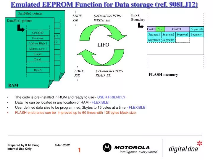
Emulated EEPROM Function for Data storage (ref. 908LJ12). : LDHX $<DataFile1PTR> JSR WRITE_EE :. DataFile2 pointer. Block Boundary. DataFile1 pointer. CPUSPD. Control. Control. Size. Segment0. Data Size. CPUSPD. Segment1. Segment2. Segment3. Segment4. Address High 2.

E N D
Emulated EEPROM Function for Data storage (ref. 908LJ12) : LDHX $<DataFile1PTR> JSR WRITE_EE : DataFile2 pointer Block Boundary DataFile1 pointer CPUSPD Control Control Size Segment0 Data Size CPUSPD Segment1 Segment2 Segment3 Segment4 Address High 2 Data Size Segment5 Segment6 Address Low 2 LIFO Address High 1 Data0 Address Low 1 Data1 Data0 Data1 DataN : LDHX $<DataFile1PTR> JSR READ_EE : DataN FLASH memory RAM • The code is pre-installed in ROM and ready to use - USER FRIENDLY! • Data file can be located in any location of RAM - FLEXIBLE! • User defined data size to be programmed, 2bytes to 15 bytes at a time - FLEXIBLE! • FLASH endurance can be improved up to 60 times with 128 bytes block size. 1
In Circuit Flash Programming Platform (ref. 908LJ12) DataFile1 pointer DataFile2 pointer CPUSPD CPUSPD Data Size Data Size Address High 1 Address High 1 Address Low 1 Address Low 1 Data0 Data0 Data1 Data1 DataN DataN PROGRAM VERIFY FLASH : LDHX $<DataFile1PTR> JSR PRGRNGE : : LDHX $<DataFile2PTR> JSR LDRNGE : RAM RAM 2
Start ISP? Execute User Code Disable COP. Exec. ISP Routine Application System TXD RXD SCI 68HC908 MCU RS232 MC145407 HC908 Flash In System Programming through SCI Port The window s/w allow user - Load/Upload data from MCU - Erase/Program/Verify Flash Memory 3
Application Software FLASH Data $0000 I/O Registers $0040 RAM $023F FLASH Programming Algorithm SCI TxD RxD PTA0 $8000 FLASH Erase FLASH Programming and erasing of FLASH locations cannot be performed by code being executed from the FLASH memory ISP Routine $FE00 Registers Monitor ROM $FFFF Vectors HC908 Flash In System Programming through SCI Port 4
In-Circuit Programming system configuration • In-System Programming is a process by which the device is programmed or erased with the device on the final end target system without open the case of the system. Target System Personal Computer Interface Board OSC_1 Additional H/W: - Header x 1 pcs - Diode x 2 pcs - Resistor - HC4066* x 1 pcs Software - MCUscribe - ICS08 M68SPGMR08 OSC_SEL* PA0 RS232 VPP VCC_S GND It may be some different control signals between interface board and target system depends on different application Example: GP32 and MR24/32 ICP Reference Demo board use 4 wires (PA0, Vpp, Vcc_s and GND). Remark: OSC_SEL and HC4066 is used when the oscillation frequency of target system is not equal to the oscillation frequency which required to entry to the monitor mode of the MCU. 5
GP32 In-Circuit Programming Reference Demo GP32 Target board simulates a typical application, user running code will be executed after provided the power to the board (rurns the LED on and off repeatedly) Remove the Target Board power and then upgrade the firmware through four wires and SPGMR with PC 6