Download
1 / 26
270 likes | 515 Vues
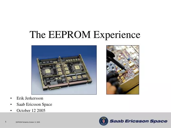
Erik Jerkersson Saab Ericsson Space October 12 2005. The EEPROM Experience.

E N D
Erik Jerkersson Saab Ericsson Space October 12 2005 The EEPROM Experience
In the frame of the IASI project several problems related to the EEPROM MEM8129 have been encountered. Since several manufacturer are using the same die in the devices these problems are also relevant to them. Outline Company presentation IASI presentation Wear out Signal integrity Software Data Protection Malicious software Conclusion BACKGROUND
Saab Ericsson Space Company Presentation Mission: Cassini/Huygens
Locations Austrian Aerospace, Vienna, Austria Headquarters: Göteborg, Sweden Mechanical Products Division, Linköping, Sweden Austrian Aerospace,Berndorf, Austria Saab Ericsson Space Inc.Los Angeles, USA
Sales 2004 - Product Areas 4 % 4 % 9 % Ground support equipment 9 % Thermal components Others 7% 11 % 11 % 46 % Antenna systems Digital Products 12 % 11 % Microwave electronics Total sales 2004 Saab Ericsson Space Group: 669 MSEK [ 91 MUSD / 73 M€ ] Mechanical systems
Resources Personnel Employees: 524, engineers University Degree or higher 54 %,engineers 40 %,others 6 % Design Tools State-of-art tools for design and analysis:- digital electronics - microwave electronics- antenna design - mechanical / thermal design Clean Rooms 3000 m² for electronics production in Göteborg, class 100 000 and class 10 000 for hybrid production 200m² for electronics production in Vienna, class 100 000 300 m² for thermal hardwareproduction in Berndorf, class 10 000 400 m² for mechanical systems and satellite integration in Linköping, class 100 000 Manufacturing 110 manufacturing operatorsMultichip Module TechnologiesSurface Mount TechnologiesPlated Through Hole TechnologiesComposite manufacturing Test 7 antenna test ranges4 thermal vacuum chambers (+1 in Vienna)2 vibrators (+1 in Vienna)Components and Materials laboratory
Digital Products Command and Data Handling Systems for more than 80 satellites in telecom, Science and earth observation applications. Guidance and Control for more than 160 Ariane launchers and now also for Vega! Payload Processing and Control for Inmarsat, Galileosat, Envisat, Metop... Instrument Applications Radio occultation GRAS, GPSOS
The IASI system aims at observing and measuring the spectrum of infrared radiation from the Earth Profiles of temperature in the troposphere Profiles of water vapour in the troposphere Ozonemeasurements Cloud top temperature/pressure Sea and land temperatures 2 IASIInfrared Atmospheric SoundingInterferometer METOP satellite
3 WEAR OUT • During the design phase a test pattern 0x80, 0x7F, …0x00, was repeatedly written to a small memory area. • Months later the EEPROM area was programmed to first 0x000000000000 and then 0xFFFFFFFFFFFF. • After a while, within minutes to several hours, more and more bits started to change from ‘1’ to ‘0’ and finally the old test pattern was visible in the memory.
It was found that temperature had an immediate effect on the data retention on these overexposed devices. Cooling the device speeded up the process to “forget” Heating helped the EEPROM to “remember” the data stored inside. • This figure shows a degrading ‘1’ with respect to time and temperature. • The waveform is remarkably the same as for a failing ‘0’ due to a weak cell. • Lesson learned - respect data sheet requirement of less than 10000 writes in page mode or 1000 in byte mode. Keep track of the number of write/erase cycles executed. Figure 1 Degrading bit
4 SIGNAL INTEGRITY • EEPROMs are known to be very sensitive to noise on the control signals. • Noise may trigger the internal state machine and the internal write cycle is started with corrupted content as consequence. • This is also true EVEN if the EEPROMs are locked. • It is often seen that the erroneous addresses are distributed in groups of 8 consecutive addresses (sub page corruption). • According to Hitachi, the manufacturer of the die, the least amount of data that is ever written in the EEPROM is a sub page consisting of just 8 consecutive addresses.
To characterise the noise sensitivity on the EEPROMs used in the IASI project several experiments where carried out on the bread board. Write strobe frequency dependency Write strobe Pulses Perturbation on Write strobe Reset signal oscillation Buffer driving EEPROM All EEPROMs were locked by the software protection algorithm all the time during these experiments. Due to the low numbers (12) of devices included in the test it is not wise to generalize the result. The result listed below could be different with another set of EEPROMs. Experiments in the IASI projectNoise sensitivity
Write strobe frequency dependency • The address was stable, the control signal CS_N was forced to an active state and the RD_N signal was forced to an inactive state when the WR_N was applied a signal with a constant frequency for a period of 5 minutes. • Could be repeated when WR_N was forced to an active state and having an oscillating signal on the CS_N signal. • The RD_N signal did not show this behaviour. • Software Data Protection enabled
Write strobe Pulses • Another test was performed with just one short pulse repeated with different timing. • The address was stable, the control signal CS_N was forced to an active state and the RD_N signal was forced to an inactive state when the WR_N was applied a signal according to the figure. • Software Data Protection enabled
Perturbation on Write strobe • The test was done with a pulse generator generating an ordinary write pulse of width 275 ns followed by none, one or two short pulses of width 12.5 ns. This was repeated every 12.5 ms during the 5 minutes long test. • WR_N was applied a signal according to the figure. • Software Data Protection enabled • It was found EEPROMs are sensitive to disturbances on the write strobe of at least two pulses at the end of the write cycle. This may be the result from the internal noise filter in the EEPROM which will filter out noise < 20 ns. Two short pulses of 12.5 ns will pass the filter and affect the EEPROM undesirably.
To characterise the EEPROM sensitivity to different frequencies applied to the reset signal a frequency generator was used. The address was stable, the CS_N was forced to active and the WR_N and RD_N were forced inactive when the disturbance was applied on the reset signal. The disturbance was applied for 5 minutes in each test. No indication of sensitivity to disturbances on the reset signal was found. Reset signal oscillation
If buffers are used for driving the EEPROM control signals, precaution has to be taken if the input signals to the buffers are left floating at any time. The output of the buffers may start to oscillate during this period and by this affect the EEPROMs in an undesired way. This floating of signals could be the case in a system where the CPU leaves the control to another master during DMA. Signals could be floating with voltage slowly decreasing during the transaction for a short period of time. Enough time for the buffers to start oscillating. Buffer driving EEPROM
Buffer driving EEPROM Figure 4 Example of oscillating EEPROM signal when the driver is tristated
It is easy to believe that the EEPROMs are not affected by an ordinary write access if they are in the locked state, but this is wrong. Even if an EEPROM is locked a write access will trigger the internal write cycle, however without writing anything (provided all timing is ok). This will cause the EEPROM not to be accessible for reading up to 10 ms. Any read during this time will give undefined data (there will be a pattern but origin of pattern found is not within scope of investigation). This phenomenon is not mentioned in the data sheet 5 SOFTWARE DATA PROTECTION
IASI software data protection experience Figure 6 Start up sequence • An ASIC will be commanded from ground to perform either patch or dump of the memory area. • The ASIC controls the DSP through JTAG. • Because of a bug in the ASIC the first DMA access might be erroneous causing an unintentional write access to the EEPROMs or RAM. • To overcome a potential dangerous write access to application SW in RAM the system performs a dummy DMA after powering up and then after a new reset is issued reloading the SW from EEPROM into RAM.
We now have learned the hard way that it is essential to wait more than 10 ms before the second start-up sequence is launched to let the EEPROM recover from a potential write access. In the beginning we thought that enabling the Software Data protection was enough. So, while running code in EEPROM, only one tiny wrong write access to the EEPROM and you will found yourself in the hot water! IASI software data protection experience (cont.)
EEPROM sensitivity to noise we now are aware of. We will now address a similar phenomenon – dangerous signals may be generated just by running SW. Data sheet states “With the software data protection enabled the entire memory array is protected from unintentional writes due to noise on the control inputs or minor bus contentions”. Data sheet also states “By using only the three byte sequence rather than the six byte sequence, the user is assured that the Software Data Protection is always enabled and that inadvertent writes will not corrupt the data in memory”. High speed processors and SW without control are a potential danger when used in a system together with EEPROM. 6 MALICIOUS SOFTWARE
If the SW is performing writes to the EEPROM without respecting the data sheet timing requirement the content may be corrupted in a way similar to the one described earlier (sub page corruption). This could be the case if the SW for some reason is crashing and running wild without any control. In the frame of the IASI project an investigation in this matter was performed and it was clear that the EEPROM is sensitive to usage outside the data sheet recommendations. The behaviour of the EEPROM varied depending on whether the EEPROM was in the locked or unlocked mode.
Not respecting the data hold time when writing to the EEPROM will only affect ongoing writes and will not cause any sub page corruption. Not respecting the 10 ms delay when writing to the EEPROM and crossing a page boundary is DANGEROUS to the EEPROM and might result in sub page corruption. Not respecting the timing of the byte load cycle will not cause any sub page corruption. Violating the byte load window timing requirement may only affect the page which was written. “Byte load window” is the time to wait after the last EEPROM specific write pulse to the next write pulse (100us). “Byte load cycle” is the time between subsequent write accesses in page mode (0.55-30us). “Write cycle time” is the EEPROM internal write cycle (10ms). Malicious SW - unlocked EEPROM
The only thing that could corrupt the content in the EEPROM was if the SW performed write accesses to the EEPROM continuously (5 seconds in the test). The minimum required time has not been investigated. The dangerous pulse width on WR_N was found to be below 100 ns. This corresponds well to the behaviour described earlier under the heading Signal integrity. A short pulse on WR_N could occur if the SW does not respect the number of wait states required. Normal write pulse width had no dangerous effect. Malicious SW - locked EEPROM
Use the page mode programming method and keep track of the number of write/erase cycles executed. It is essential to have clean and noiseless EEPROM control signals. In a design, avoid floating signals as input to buffers, which can lead to oscillation on the outputs of the buffers. If an oscillating buffer is driving EEPROM signals it can corrupt the EEPROM contents. EEPROM is affected by a write access and will be unavailable for 10 ms even if the Software Data Protection is enabled. Be aware of malicious SW. Always respect timing stated in the data sheet. Make sure the SW designer knows the EEPROM user constraints. Have the EEPROM locked. 7 CONCLUSIONS