Download
1 / 35
400 likes | 722 Vues
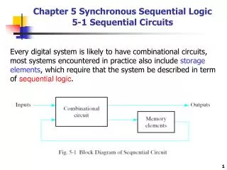
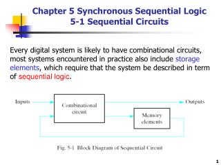
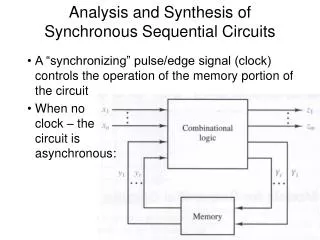
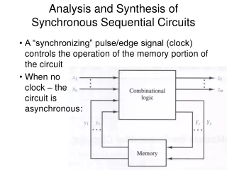
Introduction to Synchronous Sequential Circuits and Iterative Networks. Sequential Circuits and Finite-state Machines. Sequential circuit : its outputs a function of external inputs as well as stored information

E N D
Introduction to Synchronous Sequential Circuits and Iterative Networks
Sequential Circuits and Finite-state Machines Sequential circuit:itsoutputs a function of external inputs as well as stored information Finite-state machine (FSM): abstract model to describe the synchronous sequential machine and its spatial counterpart, the iterative network Serial binary adder example: block diagram, addition process, state table and state diagram
State Assignment Device with two states capable of storing information: delay element with input Y and output y • Two states:y = 0 and y = 1 • Since the present input value Y of the delay element is equal to its next output value: the input value is referred to as the next state of the delay • Y(t) = y(t+1) Example: assign state y = 0 to state A of the adder and y = 1 to B • The value of y at ti corresponds to the value of the carry generated at ti-1 • Process of assigning the states of a physical device to the states of the serial adder: called state assignment • Output value y:referred to as the state variable • Transition/output table for the serial adder: Y = x1x2 + x1y + x2y z = x1 x2 y
FSM: Definitions FSMs: whose past histories can affect their future behavior in only a finite number of ways • Serial adder: its response to the signals at time t is only a function of these signals and the value of the carry at t-1 • Thus, its input histories can be grouped into just two classes: those resulting in a 1 carry and those resulting in a 0 carry at t • Thus, every finite-state machine contains a finite number of memory devices: which store the information regarding the past input history
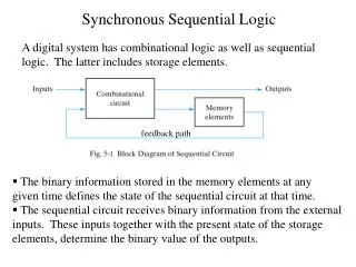
Synchronous Sequential Machines Input variables: {x1, x2, .., xl} Input configuration, symbol, pattern or vector: ordered l-tuple of 0’s and 1’s Input alphabet: set of p = 2l distinct input patterns • Thus, input alphabet I = {I1, I2, .., Ip} • Example: for two variables x1 and x2 • I = {00, 01, 10, 11} Output variables: {z1, z2, .., zm} Output configuration, symbol, pattern or vector: ordered m-tuple of 0’s and 1’s Output alphabet: set of q = 2m distinct output patterns • Thus, output alphabet O = {O1, O2, .., Oq}
Synchronous Sequential Machines (Contd.) Set of state variables: {y1, y2, .., yk} Present state: combination of values at the outputs of k memory elements Set S of n = 2kk-tuples: entire set of states S = {S1, S2, .., Sn} Next state: values of Y’s Synchronization achieved by means of clock pulses feeding the memory devices Initial state: state of the machine before the application of an input sequence to it Final state: state of the machine after the application of the input sequence
Memory Elements and Their Excitation Functions To generate the Y’s: memory devices must be supplied with appropriate input values • Excitation functions: switching functions that describe the impact of xi’s and yj’s on the memory-element input • Excitation table: its entries are the values of the memory-element inputs Most widely used memory elements:flip-flops, which are made of latches • Latch:remains in one state indefinitely until an input signals directs it to do otherwise Set-reset of SR latch:
SR Latch (Contd.) Excitation characteristics and requirements: Clocked SR latch: all state changes synchronized to clock pulses • Restrictions placed on the length and frequency of clock pulses: so that the circuit changes state no more than once for each clock pulse
Trigger or T Latch Value 1 applied to its input triggers the latch to change state Excitations requirements: y(t+1) = Ty’(t) + T’y(t) = T y(t)
The JK Latch Unlike the SR latch, J = K = 1 is permitted: when it occurs, the latch acts like a trigger and switches to the complement state Excitation requirements:
The D Latch The next state of the D latch is equal to its present excitation: y(t+1) = D(t)
Clock Timing Clocked latch: changes state only in synchronization with the clock pulse and no more than once during each occurrence of the clock pulse Duration of clock pulse: determined by circuit delays and signal propagation time through the latches • Must be long enough to allow latch to change state, and • Short enough so that the latch will not change state twice due to the same excitation Excitation of a JK latch within a sequential circuit: • Length of the clock pulse must allow the latch to generate the y’s • But should not be present when the values of the y’s have propagated through the combinational circuit
Master-slave Flip-flop Master-slave flip-flop: a type of synchronous memory element that eliminates the timing problems by isolating its inputs from its outputs Master-slave SR flip-flop: Master-slave JK flip-flop: since master-slave SR flip-flop suffers from the problem that both its inputs cannot be 1, it can be converted to a JK flip-flip
Master-slave JK Flip-flop with Additional Inputs Direct set and clear inputs: override regular input signals and clock • To set the slave output to 0: make set = 1 and clear = 0 • To set the slave output to 1: make set = 0 and clear = 1 • Assigning 0 to both set and clear: not allowed • Assigning 1 to both set and clear: normal operation • Useful in design of counters and shift registers
1’s Catching and 0’s Catching SR and JK flip-flops suffer from 1’s catching and 0’s catching Master latch is transparent when the clock is high • When the output of the slave latch is at 0 and the J input has a static-0 hazard (a transient glitch to 1) after the clock has gone high: then the master latch catches this set condition • It then passes the 1 to the slave latch when the clock goes low • Similarly, when the output of the slave latch is at 1 and the K input has a static-0 hazard after the clock has gone high: then the master latch catches this reset condition • It then passes the 0 to the slave latch when the clock goes low
D flip-flop Master-slave D flip-flop avoids the above problem: even when a static hazard occurs at the D input when the clock is high, the output of the master latch reverts to its old value when the glitch goes away
Edge-triggered Flip-flop Positive (negative) edge-triggered D flip-flip: stores the value at the D input when the clock makes a 0 -> 1 (1 -> 0) transition • Any change at the D input after the clock has made a transition does not have any effect on the value stored in the flip-flop A negative edge-triggered D flip-flop: • When the clock is high, the output of the bottommost (topmost) NOR gate is at D’ (D), whereas the S-R inputs of the output latch are at 0, causing it to hold previous value • When the clock goes low, the value from the bottommost (topmost) NOR gate gets transferred as D (D’) to the S (R) input of the output latch • Thus, output latch stores the value of D • If there is a change in the value of the D input after the clock has made its transition, the bottommost NOR gate attains value 0 • However, this cannot change the SR inputs of the output latch
Synthesis of Synchronous Sequential Circuits Main steps: • From a word description of the problem, form a state diagram or table • Check the table to determine if it contains any redundant states • If so, remove them (Chapter 10) • Select a state assignment and determine the type of memory elements • Derive transition and output tables • Derive an excitation table and obtain excitation and output functions from their respective tables • Draw a circuit diagram
Sequence Detector One-input/one-output sequence detector: produces output value 1 every time sequence 0101 is detected, else 0 • Example: 010101 -> 000101 State diagram and state table: Transition and output tables:
Sequence Detector (Contd.) Excitation and output maps: Logic diagram: z = xy1y2’ y1 = x’y1y2 + xy1’y2 + xy1y2’ y2 = y1y2’ + x’y1’ + y1’y2
Sequence Detector (Contd.) Another state assignment: z = xy1y2 Y1 = x’y1y2’ + xy2 Y2 = x’
Binary Counter One-input/one-output modulo-8 binary counter: produces output value 1 for every eighth input 1 value State diagram and state table:
Binary Counter (Contd.) Transition and output tables: Excitation table for T flip-flops and logic diagram: T1 = x T2 = xy1 T3 = xy1y2 z = xy1y2y3
Implementing the Counter with SR Flip-flops Transition and output tables: Excitation table for SR flip-flops and logic diagram: • Trivially extensible to modulo-16 counter S1 = xy1’ R1 = xy1 S2 = xy1y2’ R2 = xy1y2 S3 = xy1y2y3’ R3 = z = xy1y2y3
Parity-bit Generator Serial parity-bit generator: receives coded messages and adds a parity bit to every m-bit message • Assume m = 3 and even parity State diagram and state table: J1 = y2 K1 = y2’ J2 = y1’ K2 = y1 J3 = xy1’ + xy2 K3 = x + y2’ z = y2’y3
Sequential Circuit as a Control Element Control element: streamlines computation by providing appropriate control signals Example: digital system that computes the value of (4a + b) modulo 16 • a, b: four-bit binary number • X: register containing four flip-flops • x: number stored in X • Register can be loaded with: either b or a + x • Addition performed by: a four-bit parallel adder • K: modulo-4 binary counter, whose output L equals 1 whenever the count is 3 modulo 4
Example (Contd.) Sequential circuit M: • Input u: initiates computation • Input L: gives the count of K • Outputs: , , , z • When = 1: contents of b transferred to X • When = 1: values of x and a added and transferred back to X • When = 1: count of K increased by 1 • z = 1: whenever final result available in X
Example (Contd.) Sequential circuit M: • K, u, z: initially at 0 • When u = 1: computation starts by setting = 1 • Causes b to be loaded into X • To add a to x: set = 1 and = 1 to keep track of the number of times a has been added to x • After four such additions:z = 1 and the computation is complete • At this point:K = 0 to be ready for the next computation State diagram:
Example (Contd.) State assignment, transition table, maps and logic diagram: = y1’y2 = = y1y2 z = y1y2’ Y1 = y2 Y2 = y1’y2 + uy1’ + L’y2
A Computing Machine FSMs: called non-writing since they cannot write or change their input symbols Turing machine: FSM coupled through a head to an arbitrarily long storage register, called the tape • Tape divided into squares: each square stores a single symbol at any moment – blank squares store 0 • Head can perform three operations: reading, writing, and shifting • FSM:control unit – specifies the operations to be executed by the head • Cycle of computation:machine starts in some state Si, reads the symbol currently being scanned by the head, writes a new symbol there, shifts right or left, and then enters state Sj
Computation Example Example: initial pattern on the tape – two finite blocks of 1’s separated by a finite block of blanks • Shift the left-hand block of 1’s to the right: until it touches the right-hand block, and then halt
Turing Machine vs. Finite-state Machine Turing machine is more powerful: it can execute computations that cannot be accomplished by any FSM • Result of the Turing machine’s ability to change its input symbols • Each finite-state control unit given access to an arbitrarily large external memory in which: • it stores partial results • modifies and replaces input information • stores the output pattern • halts • Model useful for studying the capabilities and limitations of: • physical computing machines • nature of computations • type of functions not computable by any realizable machine
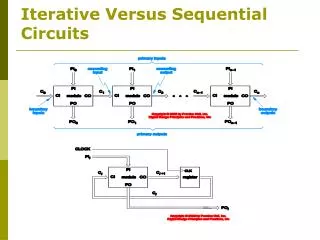
Iterative Networks Iterative network: cascade of identical cells • Sequential: counter, shift register • Combinational Every finite output sequence that can be produced sequentially by an FSM can also be produced spatially (or simultaneously) by a combinational iterative network Analogy between iterative networks and sequential machines: • Cell inputs/outputs • Input/output carries
Cell Table Cell table: analogous to state table Example: 0101 pattern detector • Assuming the same assignment for states (A: 00, B: 01, C: 11, D: 10): each cell same as the combinational logic of the sequential circuit derived for the 0101 sequence detector earlier
Synthesis Example: synthesize an n-cell iterative network • Each cell has one cell input xi and one cell output zi • zi = 1: if and only if either one or two of the cell inputs x1, x2, …, xi have value 1 • States A, B, C, D: 0, 1, 2, (3 or more) of the cell inputs to preceding cells have value 1 Cell table Cell Output-carries and cell-output table