Download
1 / 27
270 likes | 867 Vues
Analog Electronics Tutorial Series DIODES. Kristin Ackerson, Virginia Tech EE Spring 2002. Table of Contents. What are diodes made out of?____________________slide 3 N-type material_________________________________slide 4 P-type material_________________________________slide 5

E N D
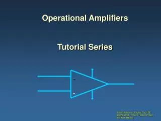
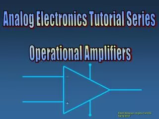
Analog Electronics Tutorial Series DIODES Kristin Ackerson, Virginia Tech EE Spring 2002
Table of Contents What are diodes made out of?____________________slide 3 N-type material_________________________________slide 4 P-type material_________________________________slide 5 The pn junction_________________________________slides 6-7 The biased pn junction___________________________slides 8-9 Properties of diodes_____________________________slides 10-11 Diode Circuit Models ____________________________slides 12-16 The Q Point____________________________________slides 17-18 Dynamic Resistance_____________________________slides 19-20 Types of diodes and their uses ___________________ slides 21-24 Sources_______________________________________slide 25 Kristin Ackerson, Virginia Tech EE Spring 2002
What Are Diodes Made Out Of? Si +4 Si +4 Si +4 Si +4 Si +4 Si +4 Si +4 Si +4 Si +4 • Silicon (Si) and Germanium (Ge) are the two most common single elements that are used to make Diodes. A compound that is commonly used is Gallium Arsenide (GaAs), especially in the case of LEDs because of it’s large bandgap. • Silicon and Germanium are both group 4 elements, meaning they have 4 valence electrons. Their structure allows them to grow in a shape called the diamond lattice. • Gallium is a group 3 element while Arsenide is a group 5 element. When put together as a compound, GaAs creates a zincblend lattice structure. • In both the diamond lattice and zincblend lattice, each atom shares its valence electrons with its four closest neighbors. This sharing of electrons is what ultimately allows diodes to be build. When dopants from groups 3 or 5 (in most cases) are added to Si, Ge or GaAs it changes the properties of the material so we are able to make the P- and N-type materials that become the diode. The diagram above shows the 2D structure of the Si crystal. The light green lines represent the electronic bonds made when the valence electrons are shared. Each Si atom shares one electron with each of its four closest neighbors so that its valence band will have a full 8 electrons. Kristin Ackerson, Virginia Tech EE Spring 2002
N-Type Material N-Type Material: When extra valence electrons are introduced into a material such as silicon an n-type material is produced. The extra valence electrons are introduced by putting impurities or dopants into the silicon. The dopants used to create an n-type material are Group V elements. The most commonly used dopants from Group V are arsenic, antimony and phosphorus. The 2D diagram to the left shows the extra electron that will be present when a Group V dopant is introduced to a material such as silicon. This extra electron is very mobile. +4 +4 +4 +4 +5 +4 +4 +4 +4 Kristin Ackerson, Virginia Tech EE Spring 2002
P-Type Material P-Type Material: P-type material is produced when the dopant that is introduced is from Group III. Group III elements have only 3 valence electrons and therefore there is an electron missing. This creates a hole (h+), or a positive charge that can move around in the material. Commonly used Group III dopants are aluminum, boron, and gallium. The 2D diagram to the left shows the hole that will be present when a Group III dopant is introduced to a material such as silicon. This hole is quite mobile in the same way the extra electron is mobile in a n-type material. +4 +4 +4 +4 +3 +4 +4 +4 +4 Kristin Ackerson, Virginia Tech EE Spring 2002
The PN Junction Steady State1 Metallurgical Junction Na Nd - - - - - - - - - - - - - - - - - - - - - - - - - - - - - - + + + + + + + + + + + + + + + + + + + + + + + + + + + + + + P n Space Charge Region ionized acceptors ionized donors E-Field + + _ _ h+ drift = h+ diffusion e- diffusion = e- drift Kristin Ackerson, Virginia Tech EE Spring 2002
The PN Junction Metallurgical Junction Na Nd + + + + + + + + + + + + + + + + + + + + - - - - - - - - - - - - - - - - - - - - P n Space Charge Region ionized acceptors ionized donors E-Field + + _ _ = = = e- drift h+ drift = h+ diffusion e- diffusion Steady State When no external source is connected to the pn junction, diffusion and drift balance each other out for both the holes and electrons Space Charge Region:Also called the depletion region. This region includes the net positively and negatively charged regions. The space charge region does not have any free carriers. The width of the space charge region is denoted by W in pn junction formula’s. Metallurgical Junction:The interface where the p- and n-type materials meet. Na & Nd:Represent the amount of negative and positive doping in number of carriers per centimeter cubed. Usually in the range of 1015 to 1020. Kristin Ackerson, Virginia Tech EE Spring 2002
The Biased PN Junction Metal Contact “Ohmic Contact” (Rs~0) _ + Applied Electric Field P n I _ + Vapplied The pn junction is considered biased when an external voltage is applied. There are two types of biasing: Forward bias and Reverse bias. These are described on then next slide. Kristin Ackerson, Virginia Tech EE Spring 2002
The Biased PN Junction Forward Bias: In forward bias the depletion region shrinks slightly in width. With this shrinking the energy required for charge carriers to cross the depletion region decreases exponentially. Therefore, as the applied voltage increases, current starts to flow across the junction. The barrier potential of the diode is the voltage at which appreciable current starts to flow through the diode. The barrier potential varies for different materials. Vapplied > 0 Reverse Bias: Under reverse bias the depletion region widens. This causes the electric field produced by the ions to cancel out the applied reverse bias voltage. A small leakage current, Is (saturation current) flows under reverse bias conditions. This saturation current is made up of electron-hole pairs being produced in the depletion region. Saturation current is sometimes referred to as scale current because of it’s relationship to junction temperature. Vapplied < 0 Kristin Ackerson, Virginia Tech EE Spring 2002
Properties of Diodes ID (mA) IS VBR VD ~V (nA) Figure 1.10 – The Diode Transconductance Curve2 • VD = Bias Voltage • ID = Current through Diode. ID is Negative for Reverse Bias and Positive for Forward Bias • IS = Saturation Current • VBR = Breakdown Voltage • V = Barrier Potential Voltage Kristin Ackerson, Virginia Tech EE Spring 2002
Properties of Diodes The Shockley Equation • The transconductance curve on the previous slide is characterized by the following equation: • ID = IS(eVD/VT – 1) • As described in the last slide, ID is the current through the diode, IS is the saturation current and VD is the applied biasing voltage. • VT is the thermal equivalent voltage and is approximately 26 mV at room temperature. The equation to find VT at various temperatures is: • VT = kT • q • k = 1.38 x 10⁻²³ J/K T = temperature in Kelvin q = 1.6 x 10⁻¹⁹ C • is the emission coefficient for the diode. It is determined by the way the diode is constructed. It somewhat varies with diode current. For a silicon diode is around 2 for low currents and goes down to about 1 at higher currents Kristin Ackerson, Virginia Tech EE Spring 2002
Properties of Diodes MathCAD Example - Application
Diode Circuit Models The Ideal Diode Model The diode is designed to allow current to flow in only one direction. The perfect diode would be a perfect conductor in one direction (forward bias) and a perfect insulator in the other direction (reverse bias). In many situations, using the ideal diode approximation is acceptable. Example: Assume the diode in the circuit below is ideal. Determine the value of ID if a) VA = 5 volts (forward bias) and b) VA = -5 volts (reverse bias) a) With VA > 0 the diode is in forward bias and is acting like a perfect conductor so: ID = VA/RS = 5 V / 50 = 100 mA b) With VA < 0 the diode is in reverse bias and is acting like a perfect insulator, therefore no current can flow and ID = 0. RS = 50 ID + VA _ Kristin Ackerson, Virginia Tech EE Spring 2002
Diode Circuit Models The Ideal Diode with Barrier Potential This model is more accurate than the simple ideal diode model because it includes the approximate barrier potential voltage. Remember the barrier potential voltage is the voltage at which appreciable current starts to flow. + V Example: To be more accurate than just using the ideal diode model include the barrier potential. Assume V = 0.3 volts (typical for a germanium diode) Determine the value of ID if VA = 5 volts (forward bias). RS = 50 With VA > 0 the diode is in forward bias and is acting like a perfect conductor so write a KVL equation to find ID: 0 = VA – IDRS - V ID = VA - V = 4.7 V = 94 mA RS50 ID + VA _ + V Kristin Ackerson, Virginia Tech EE Spring 2002
Diode Circuit Models The Ideal Diode with Barrier Potential and Linear Forward Resistance This model is the most accurate of the three. It includes a linear forward resistance that is calculated from the slope of the linear portion of the transconductance curve. However, this is usually not necessary since the RF (forward resistance) value is pretty constant. For low-power germanium and silicon diodes the RF value is usually in the 2 to 5 ohms range, while higher power diodes have a RF value closer to 1 ohm. ID + V RF Linear Portion of transconductance curve RF = VD ID ID VD VD Kristin Ackerson, Virginia Tech EE Spring 2002
Diode Circuit Models The Ideal Diode with Barrier Potential and Linear Forward Resistance Example: Assume the diode is a low-power diode with a forward resistance value of 5 ohms. The barrier potential voltage is still: V = 0.3 volts (typical for a germanium diode) Determine the value of ID if VA = 5 volts. RS = 50 Once again, write a KVL equation for the circuit: 0 = VA – IDRS - V - IDRF ID = VA - V = 5 – 0.3 = 85.5 mA RS + RF 50 + 5 ID + VA _ + V RF Kristin Ackerson, Virginia Tech EE Spring 2002
Diode Circuit Models Values of ID for the Three Different Diode Circuit Models These are the values found in the examples on previous slides where the applied voltage was 5 volts, the barrier potential was 0.3 volts and the linear forward resistance value was assumed to be 5 ohms. Kristin Ackerson, Virginia Tech EE Spring 2002
The Q Point The operating point or Q point of the diode is the quiescent or no-signal condition. The Q point is obtained graphically and is really only needed when the applied voltage is very close to the diode’s barrier potential voltage. The example 3 below that is continued on the next slide, shows how the Q point is determined using the transconductance curve and the load line. First the load line is found by substituting in different values of V into the equation for ID using the ideal diode with barrier potential model for the diode. With RS at 1000 ohms the value of RF wouldn’t have much impact on the results. ID = VA – V RS Using V values of 0 volts and 1.4 volts we obtain ID values of 6 mA and 4.6 mA respectively. Next we will draw the line connecting these two points on the graph with the transconductance curve. This line is the load line. RS = 1000 ID + VA = 6V _ + V Kristin Ackerson, Virginia Tech EE Spring 2002
The Q Point The transconductance curve below is for a Silicon diode. The Q point in this example is located at 0.7 V and 5.3 mA. ID(mA) 12 10 8 Q Point: The intersection of the load line and the transconductance curve. 6 5.3 4.6 4 2 VD(Volts) 0.2 0.4 0.6 0.8 1.0 1.2 1.4 0.7 Kristin Ackerson, Virginia Tech EE Spring 2002
Capacitance and Voltage of PN Junctions Diode Operation – Animation Webpage Link
Dynamic Resistance The dynamic resistance of the diode is mathematically determined as the inverse of the slope of the transconductance curve. Therefore, the equation for dynamic resistance is: rF = VT ID The dynamic resistance is used in determining the voltage drop across the diode in the situation where a voltage source is supplying a sinusoidal signal with a dc offset. The ac component of the diode voltage is found using the following equation: vF = vac rF rF + RS The voltage drop through the diode is a combination of the ac and dc components and is equal to: VD = V + vF Kristin Ackerson, Virginia Tech EE Spring 2002
Dynamic Resistance Example: Use the same circuit used for the Q point example but change the voltage source so it is an ac source with a dc offset. The source voltage is now, vin = 6 + sin(wt) Volts. It is a silicon diode so the barrier potential voltage is still 0.7 volts. The DC component of the circuit is the same as the previous example and therefore ID = 6V – 0.7 V = 5.2 mA 1000 rF = VT = 1 * 26 mV = 4.9 ID 5.3 mA = 1 is a good approximation if the dc current is greater than 1 mA as it is in this example. RS = 1000 ID + vin + V vF = vac rF = sin(wt) V 4.9 = 4.88 sin(wt) mV rF + RS 4.9 + 1000 Therefore, VD = 700 + 4.9 sin (wt) mV (the voltage drop across the diode) Kristin Ackerson, Virginia Tech EE Spring 2002
Types of Diodes and Their Uses PN Junction Diodes: Are used to allow current to flow in one direction while blocking current flow in the opposite direction. The pn junction diode is the typical diode that has been used in the previous circuits. A K P n Schematic Symbol for a PN Junction Diode Representative Structure for a PN Junction Diode Zener Diodes: Are specifically designed to operate under reverse breakdown conditions. These diodes have a very accurate and specific reverse breakdown voltage. A K Schematic Symbol for a Zener Diode Kristin Ackerson, Virginia Tech EE Spring 2002
Types of Diodes and Their Uses Schottky Diodes: These diodes are designed to have a very fast switching time which makes them a great diode for digital circuit applications. They are very common in computers because of their ability to be switched on and off so quickly. A K Schematic Symbol for a Schottky Diode Shockley Diodes: The Shockley diode is a four-layer diode while other diodes are normally made with only two layers. These types of diodes are generally used to control the average power delivered to a load. A K Schematic Symbol for a four-layer Shockley Diode Kristin Ackerson, Virginia Tech EE Spring 2002
Types of Diodes and Their Uses Light-Emitting Diodes: Light-emitting diodes are designed with a very large bandgap so movement of carriers across their depletion region emits photons of light energy. Lower bandgap LEDs (Light-Emitting Diodes) emit infrared radiation, while LEDs with higher bandgap energy emit visible light. Many stop lights are now starting to use LEDs because they are extremely bright and last longer than regular bulbs for a relatively low cost. The arrows in the LED representation indicate emitted light. A K Schematic Symbol for a Light-Emitting Diode Kristin Ackerson, Virginia Tech EE Spring 2002
Types of Diodes and Their Uses Photodiodes: While LEDs emit light, Photodiodes are sensitive to received light. They are constructed so their pn junction can be exposed to the outside through a clear window or lens. In Photoconductive mode the saturation current increases in proportion to the intensity of the received light. This type of diode is used in CD players. In Photovoltaic mode, when the pn junction is exposed to a certain wavelength of light, the diode generates voltage and can be used as an energy source. This type of diode is used in the production of solar power. A K A K Schematic Symbols for Photodiodes Kristin Ackerson, Virginia Tech EE Spring 2002
Sources Dailey, Denton. Electronic Devices and Circuits, Discrete and Integrated. Prentice Hall, New Jersey: 2001. (pp 2-37, 752-753) 2 Figure 1.10. The diode transconductance curve, pg. 7 Figure 1.15. Determination of the average forward resistance of a diode, pg 11 3 Example from pages 13-14 Liou, J.J. and Yuan, J.S. Semiconductor Device Physics and Simulation. Plenum Press, New York: 1998. Neamen, Donald. Semiconductor Physics & Devices. Basic Principles. McGraw-Hill, Boston: 1997. (pp 1-15, 211-234) 1 Figure 6.2. The space charge region, the electric field, and the forces acting on the charged carriers, pg 213. Kristin Ackerson, Virginia Tech EE Spring 2002