Download
1 / 26
260 likes | 387 Vues
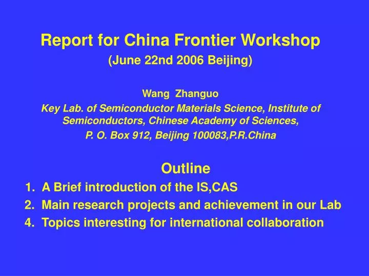
Report for China Frontier Workshop (June 22nd 2006 Beijing) Wang Zhanguo Key Lab. of Semiconductor Materials Science, Institute of Semiconductors, Chinese Academy of Sciences, P. O. Box 912, Beijing 100083,P.R.China Outline 1. A Brief introduction of the IS,CAS

E N D
Report for China Frontier Workshop (June 22nd 2006 Beijing) Wang Zhanguo Key Lab. of Semiconductor Materials Science, Institute of Semiconductors, Chinese Academy of Sciences, P. O. Box 912, Beijing 100083,P.R.China Outline 1. A Brief introduction of the IS,CAS 2. Main research projects and achievement in our Lab 4. Topics interesting for international collaboration
1.A Brief introduction of the Institute of Semiconductors, Chinese Academy of Sciences The Institute originally was a division of the Institute of Physics, CAS, and it was independent on the 16th September 1960. Through the period of more than 45 years, the Institute has now grown up a multidisciplinary research institution and research areas includes semiconductor physics, materials, devices and their applications. It has two national research centers, three state key labs, one key lab of CAS , 10 joint venture enterprises, Library and Information Center etc. Main Research Building
There are now 452 staffs in the Institute, 270 are academic staffs including 71 full professors and 62 associate professors. There are seven Members of the CAS and two Members of the CAE. The institute has 408 postgraduate students, 18 postdoctoral researchers, 233 PhD and 157 MSc students, respectively. The Integrated Technology Center Compound Crystal Technology Co., Ltd can supply LEC,VGF and HB GaAs with 2-6 inches and 2-3 inches InP Epi-ready wafers.
Molecular Beam Epitaxy system for low dimensional semiconductor structures growth:QDs and QWRs etc.
Molecular Beam Epitaxy system (V80) used for growing magnetic semiconductors
Electron Beam Lithograph system with high resolution of 10nm (left) and The functional integration Lab of optoelectronic devices (right)
2. The main research projects carried out in my group are as follows: • Semiconductor nano-structures and quantum devices • 2. Positional growth of QDs and QWRs • GaAs and InP based quantum cascade materials and lasers • Wide band-gap semiconductor thin films and nanostructures growth • Organic/inorganic composite semiconductors for solar cells • Research founding supported by NSFC, 863 Hi-Tech and 973 National Major Basic Research Program etc.
x=0.3 x=0.4 x=0.5 Lift 1 and 2 are the 2D AFM images of InxGa1-xAs QDs grown on (311)B GaAs substrates. Changing In composition x of InGaAs QDs 3D images of InxGa1-xAs / GaAs (311)B QDs (0.4 0.4mm)
a b d) c Inserting In0.5Al0.15Ga0.35As strain reducing layer between QD layer & substrate (a), (b) and (c), (d) are without and with the buried layer respectively. Comparing fig.a,b and c,d,the In0.4Ga0.6As QDs density is increased and ordering effect is improvedlargely.
Light output power from the uncoated facets vs the current EL spectra of a QD laser below and above the threshold current Characteristics of high power In(Ga)As/GaAs QDLD
Width of LD, 200mm Cavity length 600mm The samples of high power QD laser diodes 960nm10W QDLD optical fiber module
200 (a.u.) 1400mA 150 Light Output ( m W ) Intensity 100 EL 50 0 400 600 800 1000 1200 1400 900 950 1000 1050 1100 Wavelength (nm) Injection Current (mA) The Characteristics of quantum dot-SLD: CW output power 200mW, the spectral bandwidth 60nm at RT Light output power of the QD-SLD under CW operation at RT. Output spectrum of QD-SLD under 1400mA CW pumping current at RT.
The diagonally aligned self-assembled InAs/InAlAs/InP(100) QWR arrays 10nm (110) (1-10) The cross-sectional TEM images and PL spectra of 5 periods 6.5 ML InAs / 10 nm InAlAs QWR arrays.
InAs/InGaAs/InP QWRs InAs/InAlAs/InP QWRs a b 30nm InAs/[(InAlAs)2/(InGaAs)2] InAs/[(InAlAs)4/(InGaAs)2] d c The alignment of the QWRs grown on InP substrates with different buffer layers
MEE, (001), 8ML MBE, (001), 8ML MBE, (mis-oriented), 8ML MEE, (001), 10ML Symmetry in the InAs wire alignment
Lower Left fig. shows InAs QWRs grown on the (110) cleavage surface of GaAs/AlGaAs SLs Lower right fig. demonstrates the InAs QDs grown in the patterned GaAs substrates.
Operation principle of quantum cascade laser This SL has double merits: n=3’s Bragg reflector, n=1’s electron extraction. Particle population inversion based on the resonance with the optical phonon.
The lower left fig. shows the TEM result of strain-compensated In0.55Ga0.45As/In0.5Al0.5As The lower right fig. shows the XRD spectrum of 25 period In0.55Ga0.45As/In0.5Al0.5As QCL
1W QCW operation at 80K 50C脉冲激射 The output power vs current for the 5.5m strain-compensated QCL
Samples for quasi-single mode quantum cascade lasers made by our Lab. 84K 83K INTENSITY(a.u.) 800 900 1000 1100 1200 1300 1400 FREQUENCY(cm-1) 83K9.1m GaAs/AlGaAs QCL lasing spectrum 7.8m strain-compensated QCL lasing spectrum
60 Min CSI 60 Min CSI min 15 Min CSI 15 Min CSI ZnO nanostructures grown by Stress driving Fig. (a),(b) and (c),(d)are FE Cross Section Imaging at growth time of 60min and 15min respectively
3. Topics interesting for international collaboration Positional growth of semiconductor QDs and QWRs Quantum dot devices for systems applications such as: high power QD Laser, 1.3mmand 1.5mm QD lasers, super- luminescence diodes for optical fiber communication; QD inferred detectors; QD single photon source for quantum computation etc. Band energy engineering design for THz (30-300mm) structures and lasers Property studies on single QD and QWR