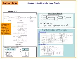
Combinatorial Logic Circuit Diagrams
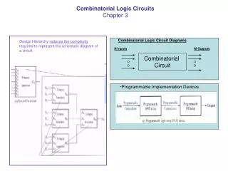
Combinatorial Logic Circuits Chapter 3. Combinatorial Logic Circuit Diagrams. Design Hierarchy reduces the complexity required to represent the schematic diagram of a circuit. N Inputs. M Outputs. Combinatorial Circuit. - Programmable Implementation Devices.

Combinatorial Logic Circuit Diagrams
E N D
Presentation Transcript
Combinatorial Logic CircuitsChapter 3 Combinatorial Logic Circuit Diagrams Design Hierarchy reduces the complexity required to represent the schematic diagram of a circuit N Inputs M Outputs Combinatorial Circuit -Programmable Implementation Devices
Combinatorial Logic CircuitsChapter 3 • The purpose of this chapter is to use the knowledge acquired in the previous chapters to formulate systematic design procedures for combinatorial circuits. • The design steps will be related to the use of computer aided design tools. In this chapter we introduce the use of a hierarchy and top down design, which are essential for the design of digital circuits. Computer Aided-Design is discussed including Hardware Description Languages (HDL’s) and Logic Synthesis. Topics related to digital circuit implementation are discussed: Fan-in Fan-out Propagation delays Design procedures are presented: Specification Formulation Optimization Fixed implementation & technology mapping Verification
Combinatorial Logic CircuitsChapter 3 A Combinatorial circuit performs an operation that can be specified by a set of Boolean equations. A Sequential circuit employ elements that store bit values. The outputs of a sequential circuit depend not only on the current input values, but also on past inputs. A combinatorial circuit consists of input variables, output variables, logic gates and interconnections. Each input and output variable consists of a binary signal that takes on values 0 and 1. For n inputs there are 2n possible binary input combinations For each binary combination of the input variables there is one possible binary value on each output specified by a truth table. N Inputs M Outputs Combinatorial Circuit A combinatorial function can also be described by m Boolean functions, one for each output variable.
Combinatorial Logic CircuitsChapter 3 • Design Hierarchy: • A circuit may be specified by a symbol showing its inputs and outputs and a description on how it operates. • A complex digital system may contain millions of interconnected gates. A Very Large Scale Integrated (VLSI) processor often contains tens of millions of gates. • In order to deal with such circuit complexity, a divide and conquer approach is used. • A circuit is broken into blocks that are interconnected to form the circuit. • The functions of blocks and their interfaces are clearly defined so the circuit obeys the circuit specification. A hierarchy gives a simplified representation of a complex circuit Circuit as 3 input odd function blocks Xo X1 X2 Ao A1 A2 3-Input odd function Xo X1 X2 X3 X4 X5 X6 X7 X8 Symbol for circuit 9 input Odd function B0 Ao A1 A2 3-Input odd function X3 X4 X5 Ao A1 A2 3-Input odd function Zo B0 Zo B0 X6 X7 X8 Ao A1 A2 3-Input odd function B0 Each EOR can be represented by 4 NAND Gates Ao A1 A2 Bo Circuit using exclusive Or’s
Combinatorial Logic CircuitsChapter 3 The Hierarchy ends in a set of leaves. In this case the leaves consist of NAND gates, referred as primitive blocks. We are only interested in designing the logic. Their function can be defined by a program or description that can serve as a model. 9-Input Odd function 3-Input Odd function 3-Input Odd function 3-Input Odd function 3-Input Odd function XOR XOR XOR XOR XOR XOR XOR XOR NAND Gates
Combinatorial Logic CircuitsChapter 3 We can simplify it even further, where there is only one copy of each block, since the designer can design one three input odd function block and one exclusive-OR block and can use these multiple times respectively. The appearance of a block within a design is called an instance of the block and its use is called instantiation. The block is reusable and this greatly reduces the design effort required for complex circuits. 9-Input Odd function 3-Input Odd function XOR
Combinatorial Logic CircuitsChapter 3 • In later chapters we focus on predefined reusable blocks. These blocks provide basic functions used in digital design. • This allows designers to do much of the design process above the primitive block level. • These blocks are in computer aided design tool libraries Top Down Design: The circuit function is specified by text or a Hardware Description Language (HDL) plus constraints on cost, performance and reliability. In automated synthesis, the HDL description is converted to logic automatically. (Ideal approach). In reality its often necessary to perform portions of the design bottom up to make maximum use of predefined modules. A particular circuit design may violate one of the constraints of the initial specification. In this case its often necessary to backtrack upward to a level at which the violation is reached.
Combinatorial Logic CircuitsChapter 3 Computer Aided Design (CAD) Designing complex systems would not be feasible without CAD tools. Libraries of graphics symbols and functional blocks are provided. The primitive and functional blocks have associated models that allow the behavior and the timing of the hierarchical blocks to be verified.
Combinatorial Logic CircuitsChapter 3 Gate Properties: An Integrated Circuit (IC) is a silicon semiconductor crystal, called a chip, containing the gates and storage elements. The chip is mounted on a ceramic or plastic container and the connections are made to the external pins. The number of pins range from 14 to several hundred on large IC’s. Each IC has a numeric designation printed on the package. Vendors publish data sheets or catalogs that describe the functional characteristics of the IC’s. Definitions: The number of gates present on a chip ranges from small scale integrated to Very Large Scale. Small scale Integrated (SSI): Contain several primitive gates usually less that 10. Medium Scale Integrated (MSI): Contain 10-100 gates: Example simple 4-bit adder: Large Scale Integrated (LSI): Contain between a 100 and several thousand gates. Example is a simple processor. Very Large Scale Integrated (VLSI): Contains several thousand to tens of millions of gates. Example is a complex microprocessor. Complementary Metal Oxide Semiconductor (CMOS): Used for high circuit density, high performance low power applications. Gallium Arsenide (GaAs) and Silicon Germanium(SiGe) are used for very high speed circuits.
Combinatorial Logic CircuitsChapter 3 Technology Parameters: Parameters used to characterize an implementation technology: Fan-in: specifies the number of inputs available on a gate. Usually restricted to 4 or 5.(related to gate speed) Fan-out: specifies the number of standard loads driven by a gate output. Maximum fan-out, specifies the fan-out that the output can drive without impairing gate performance. Noise margin: is the maximum external noise voltage superimposed on a normal input value that will not cause an undesirable change in the circuit output. Propagation Delay: Is the time required for a change in value of a signal to propagate from input to output. Power Dissipation: Is the power drawn from the power supply and consumed by the gate. The power consumed is dissipated as heat. Related to the operating temperature and cooling requirements of the chip. In The high to low propagation Tphl is the delay measured from the reference voltage IN to the reference voltage OUT In Out Tphl Tplh Out Tpd is the propagation delay = max(Tphl, Tplh) Reason for this is to find the longest time for a signal to propagate from inputs to outputs
Combinatorial Logic CircuitsChapter 3 Takes ~1 NS to go from Logical 0 to 1 A B No delay Transport Delay Time (Ns) 0 1 2 3 4 5 6 7 8 AND Gate Example of Transport and Inertial Delays
Combinatorial Logic CircuitsChapter 3 Fan-out: Each input on a given gate provides a load on the output of the driving gate which is measured in standard load units. The input to a specific inverter can have a standard load of 1.0. If a gate drives six inverters then it would be 6.0. The output of a gate has a maximum load it can drive called maximum fan-out. The load on the output of a gate determines the time required for the output of the gate to change fro H to L and L to H. If the load on the output is increased then this time transition time is increases. The propagation delay is also increased. Ex: Calculation of gate delay based on fan-out. A 4 input NAND gate output is attached to the inputs of the following gates. -4 input NOR gate 0.8 standard load -3 input NAND gate 1.0 standard load -Inverter 1.0 standard load The formula for the delay of the 4 input NAND gate is (CMOS gates) Tpd=0.07 + 0.021 X SL ns (where SL is the sum of the standard loads driven by the gate) (ignoring the wiring delay) (Tpd is the propagation delay) Tpd=0.07 + 0.021 x (0.8 + 1.0 + 1.0) = 0.129 ns
Combinatorial Logic CircuitsChapter 3 Cost: The cost is based on the area occupied by the layout cell for the circuit. The layout cell area is proportional to the size of the transistors and the wiring in the gate layout. Ignoring the wiring area, the area of the gate is proportional to the number of transistors in the gate, which is usually proportional to the gate input count. Positive and Negative Logic: Choosing the High level to represent logic 1 defines a positive-logic system. Choosing the Low level to represent logic 1 defines a negative logic system. Data sheet for CMOS gate where H=5.0 Volts L= 0.0 Volts X Y Z L L L L H L H L L H H H X Y CMOS Gate Z Truth Table Gate block diagram
Combinatorial Logic CircuitsChapter 3 X Y Z 0 0 0 0 1 0 1 0 0 1 1 1 X Y Positive Logic Z X Y Z 0 0 1 0 1 1 1 0 1 1 1 0 Negative Logic X Y Z The small triangles on the inputs and outputs arepolarityindicators , which signifies that negative logic is assumed for the corresponding signal (also called taking the dual of the gate function. We will use positive logic in the text.
Combinatorial Logic CircuitsChapter 3 Design Procedure: The design of a combinatorial circuit starts from the specification of the problem and culminates in a logic diagram (or netlist that describes a logic diagram) The procedure involves the following steps: 1) Specification: Write a specification for the circuit 2)Formulation: Derive the truth table or initial Boolean equations that define the required relationships between inputs and outputs. 3)Optimization: Apply two-level and multi-level optimization. Draw a logic diagram or netlist for the resulting circuit using AND , OR’s and Inverters. 4) Technology Mapping: Transform the logic diagram or netlist to a new diagram or netlist using available implementation Technology. Technology Mapping replaces AND, OR Gates and Inverters with gates from the technology library 5) Verification: Verify the correctness of the final design. Netlist: When using a HDL (Hardware description Language, XiLinx) a structural description describes the interconnection of components. This structural description is referred to as a netlist, used as input to a logic simulator.
Combinatorial Logic CircuitsChapter 3 Example (Design Procedure:) Design of a BCD to Excess-3 Code converter: (Add 3 to every BCD digit) • Step 1) Specification: The Excess-3 code for a decimal digit is the binary combination corresponding to the decimal digit plus 3. An example is given the decimal digit 5 the binary combination is 5+3=8 (1000). • Each BCD digit is four bits labeled A,B,C,D. • Each Excess-3 digit is four bits labeled W,X,Y,Z. Step 2) Formulation: The Excess-3 code is obtained by adding 0011 (3) to each BCD code. BCD codes 1010 through 1111 are not listed and can be treated ad don’t care conditions. DecimalInput BCD Output Excess-3 A B C DW X Y Z 0 0 0 0 00 0 1 1 1 0 0 0 10 1 0 0 2 0 0 1 00 1 0 1 3 0 0 1 10 1 1 0 4 0 1 0 00 1 1 1 5 0 1 0 11 0 0 0 6 0 1 1 01 0 0 1 7 0 1 1 11 0 1 0 8 1 0 0 01 0 1 1 9 1 0 0 11 1 0 0 A K-Map will be generated for each output variable K-Map for Y K-Map for X Truth Table: K-Map for W K-Map for Z
Combinatorial Logic CircuitsChapter 3 • Step 3: Optimization: This is a four variable function and we use the Karnaugh maps for optimization. • For each output variable W,X,Y,Z we need a separate K-Map. Truth Table for W=1 A B C D 5 0 1 0 1 = A B C D 6 0 1 1 0 = A B C D 7 0 1 1 1 = A B C D 8 1 0 0 0 = A B C D 9 1 0 0 1 = A B C D BC CD 00 01 11 10 AB BD 00 01 11 10 1 1 1 A A B C D A B C D A B C D Don’t-Care are BCD numbers 10-15 1010,1011,1100,1101,1110,1111 Optional to use these elements X X X X A B C D A B C D A B C D A B C D 1 1 X X A B C D A B C D A B C D A B C D W=A + BC + BD
Combinatorial Logic CircuitsChapter 3 • Step 3: Optimization: This is a four variable function and we use the Karnaugh maps for optimization. • For each output variable W,X,Y,Z we need a separate K-Map. Truth Table for X=1 A B C D 1 0 0 0 1 = A B C D 2 0 0 1 0 = A B C D 3 0 0 1 1 = A B C D 4 0 1 0 0 = A B C D 9 1 0 0 1 = A B C D BC BD CD 00 01 11 10 AB 1 1 1 00 01 11 10 A B C D A B C D A B C D 1 A B C D BCD X X X X A B C D A B C D A B C D A B C D 1 X X A B C D A B C D A B C D A B C D X=BC + BD + BCD
Combinatorial Logic CircuitsChapter 3 A B C D • Step 3: Optimization: This is a four variable function and we use the Karnaugh maps for optimization. • For each output variable W,X,Y,Z we need a separate K-Map. Truth Table for Y=1 • A B C D • 1 0 0 0 0 = A B C D • 3 0 0 1 1 = A B C D • 4 0 1 0 0 = A B C D • 0 1 1 1 = A B C D • 1 0 0 0 = A B C D A B C D CD 00 01 11 10 AB 1 1 00 01 11 10 A B C D 1 1 A B C D A B C D CD CD X X X X A B C D A B C D A B C D A B C D 1 X X A B C D A B C D A B C D Y=CD + CD
Combinatorial Logic CircuitsChapter 3 • Step 3: Optimization: This is a four variable function and we use the Karnaugh maps for optimization. • For each output variable W,X,Y,Z we need a separate K-Map. Truth Table for Z=1 A B C D 0 0 0 0 0 = A B C D 2 0 0 1 0 = A B C D 4 0 1 0 0 = A B C D 6 0 1 1 0 = A B C D 8 1 0 0 0 = A B C D CD 00 01 11 10 AB 1 1 00 01 11 10 A B C D A B C D 1 1 A B C D A B C D D X X X X A B C D A B C D A B C D A B C D 1 X X A B C D A B C D A B C D Z=D
Combinatorial Logic CircuitsChapter 3 Optimization (cont): Each of the four maps represents one of the outputs of the circuit. W=A + BC + BD X=BC + BD + BCD Y=CD + CD Z=D A W X B Y C D Z
Combinatorial Logic CircuitsChapter 3 Technology Mapping: Starting with an optimized circuit we develop a new circuit using common gate elements. NAND gates are often used, since we can represent other gates using them. As shown from Chapter 2: A gate type that alone can be used to implement all Boolean functions is called a Universal gate. Using a NAND gate as a AND gate X Y XY Using a NAND gate as a OR gate X Y X Y X + Y NAND Gate F=X Y X Y F • X Y X YX + Y • 0 0 1 1 0 • 0 1 1 0 1 • 0 0 1 1 • 1 1 0 0 1 X Y Z= XY 0 0 1 0 1 1 1 0 1 1 1 0
Combinatorial Logic CircuitsChapter 3 Cell Library for technology mapping: ( to NAND Logic) Cell NameCell SchematicNormalizedTypicalTypical Input toBasic Function AreaInput LoadOutput DelayTemplate Inverter 2 NAND 3 NAND 1.0 1.00 0.04 + .012 * SL (referred to as 1.0 Standard Load ) 1.25 1.00 .05 + .014 * SL 1.50 1.00 0.06 + .017 * SL Basic building block 2NAND Procedures (Replace AND-OR gates with equivalent circuits) AND OR
Combinatorial Logic CircuitsChapter 3 Using Technology MappingBCD to Excess-3 Code Converter A W B X C D Y (AOI) And –or-Inverter Z
Combinatorial Logic CircuitsChapter 3 5) Verification / Simulation: The goal is to determine whether a given circuit implements its specified function (Boolean equations and HDL are used) Original Specification Technology Mapped Circuit Result (should be same as Specification) DecInput BCD Output Excess-3 A B C DW X Y Z 0 0 0 0 00 0 1 1 1 0 0 0 10 1 0 0 2 0 0 1 00 1 0 1 3 0 0 1 10 1 1 0 4 0 1 0 00 1 1 1 5 0 1 0 11 0 0 0 6 0 1 1 01 0 0 1 7 0 1 1 11 0 1 0 8 1 0 0 01 0 1 1 9 1 0 0 11 1 0 0 A W B X C D Y (AOI) And –or-Inverter Z