Prototyping Electronic Assemblies
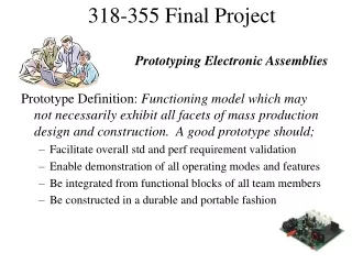
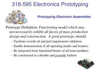
Prototyping Electronic Assemblies. Prototype Definition: Functioning model which may not necessarily exhibit all facets of mass production design and construction. A good prototype should; Facilitate overall std and perf requirement validation

Prototyping Electronic Assemblies
E N D
Presentation Transcript
Prototyping Electronic Assemblies Prototype Definition: Functioning model which may not necessarily exhibit all facets of mass production design and construction. A good prototype should; • Facilitate overall std and perf requirement validation • Enable demonstration of all operating modes and features • Be integrated from functional blocks of all team members • Be constructed in a durable and portable fashion
Basic Prototype Methods Breadboard or Plugboard Advantages • Solderless, Easy Mods • Very Rapid Prototyping • Well suited to TH 0.3” and 0.6” DIP IC’s & Low Power Discretes • Used in previous Labs Disadvantages • Holes limited to #18-22 AWG “solid” leads/wires on 0.1” centers • Circuit must be transported with extreme care • Boards are subject to wearout, wire breakages, warping, etc • Expensive, cumbersome for larger circuits • Not suited to SMT, connectors, displays, power devices, switches, etc • >10pF row-row capacitance
Basic Prototype Methods Wirewrap or Termipoint Advantages • Can be solderless or used in with solder • Relatively Rapid Prototyping • Well suited to DIP and SMT Conversions • Easy Mods but Very Reliable Disadvantages • All parts must fit into WW sockets/headers on 0.1” centers • WW Wire is small, #30 AWG, <100mA, 250nH/ft • WW Tool and special solid WW Wire required • Best Results with Pre-stripped Wire • Requires special WW sockets, bottom ID’s and perf board
Basic Prototype Methods Perfboard without Pads Advantages • Used with top or bottom side solder wire-wire connections • Can be used with DIP and SMT Conversion Sockets • Mods possible but require unsoldering • Reliable if used with hold down adhesives Disadvantages • All parts must fit into sockets/headers on 0.1” center hole pattern • Solder connections made with wire-wire or wire-pin • Insulation on wire connections can be compromised with heat • Slower than Wirewrap or solderless breadboard • Requires higher degree of soldering skills
Basic Prototype Methods Perfboard with Pads Advantages • Used with top or bottom side solder wire-wire connections • Can be used with DIP and SMT Conversion Sockets • Mods possible but require unsoldering pads (vacuum required) • Available with Gnd Planes, Power Traces/Busses • Better solder connections than w/o pads, More Reliable Disadvantages • All parts must fit into mountings on the hole pattern • More expensive than std perfboard • Slower than Wirewrap or solderless breadboard • Requires moderate degree of soldering skills
Basic Prototype Methods Deadbug Board Advantages • Access to connection side of all parts • Allows an excellent ground plane(s), Great for HF, VHF, UHF, RF • Copper board can be scraped to provide power traces as well • Inexpensive, Reliable if used with hold down adhesives Disadvantages • Part markings are upside-down • Not suited to digital or nodal intensive circuits • Requires adhesive to “deadbug” parts • Slow Method, Can be very delicate when part legs extend vertically • Requires very high degree of soldering skills
Basic Prototype Methods Printed Circuit Board – PCB Handmade – Transfer Artwork Process • Designer must utilize ruboff transfers, tape or pen hand lithography • Once design is transferred to Cu laminate, board is etched, then drilled Advantages • Mostly repeatable performance for RLC board effects • Can be used with or without component sockets, SMT or Thru Hole Parts • Relatively Fast Creation of Simple PCBs, less than 15 parts • High current capability for any conductor if properly designed • Good for power circuits, large copper area intensive circuits Disadvantages • For single or double sided boards only, No True Vias • Features less than 100mil spacing, 0805 discrete, 10mil trace very difficult • Requires use of chemical ether such as FeCl
Etching of Printed Circuits CAUTION !! Developing and etching PCBs is a process that involves chemicals that dissolve metal (etching process). These chemicals can also burn your skin, have hazardous or toxic fumes, and can be absorbed under prolonged contact. In most cased these chemicals CANNOT and SHOULD NOT be disposed of by dumping into ordinary sanitary drains. PC etching should NEVER be done without adequate ventilation or in an area accessible by children, pets or other unsuspecting persons. Also these materials may stain or discolor flooring, furniture, and clothing. Follow ALL safety cautions mentioned on any etching materials purchased.
Basic Prototype Methods Printed Circuit Board – PCB Handmade – Photolithography Process • Designer must create photo lithograph “mask” of Cu circuit using eCAD • Positive or Negative Photo Sensitive Resist Cu laminate is then exposed (printed) to lithograph design, etched and drilled Advantages • Repeatable performance for RLC board effects • Can be used with or without component sockets, SMT or Thru Hole Parts • Fast assembly once PCB is created, drilled • High current capability for any conductor if properly designed • Good for Single and Double Sided boards Disadvantages • For single or double sided boards only, No True Vias • Involved, Difficult Process involving photo process, Easy to make mistakes • Requires use of Chemical Etcher such as FeCl
Basic Prototype Methods Printed Circuit Board – PCB Outsourced Advantages • Professional, repeatable performance for RLC, mass producable • Can be used with or without component sockets, SMT or Thru Hole Parts • Fast assembly once PCB is procured • High current capability for any conductor • By far the most reliable prototype method • Circuit can be matched by computer to intended schematic Disadvantages • Procurement Time of PCB Fab takes ~1-2 weeks, (quick turn is an option) • Changes or mistake fixing can require “unsoldering” skills/tools • Extra Design Task of Creating Board Layout File/Artwork
10 Guidelines • Make good power supply and ground connections • A 30 AWG#, daisy-chained wire-wrap connection from chip to chip is very inadequate. For similar reasons to the decoupling, you must make low impedance power supply and ground returns. • For single and double sided boards use 20mil or larger (wider) traces. • For multilayer boards use separate planes for power(s) and ground(s) when possible • Check ALL wire & trace gauges for proper current capacity. • Decouple ALL IC power inputs • This includes analog, digital and data conversion IC’s • Employ a 0.1 uf ceramic capacitor from each supply to ground as close to the IC as possible. Switching internal to the IC can cause momentary voltage drops due to package and line length inductances. A local capacitor helps counteract this effect by providing local energy. • Include separate bypass capacitors for both the positive and negative supplies • Each circuit board should have additional “bulk” capacitors such as solid tantalum depending on local current draw
10 Guidelines • Keep digital and analog circuitry physically separated if possible • Digital switching, especially at microprocessor bus or video card speeds, can inject switching noise and other unwanted effects into analog circuitry. • When possible use separate analog and digital power and ground return runs, planes and/or wiring back to a central point as close to the DC power source as possible. This will keep the digital noise out of the analog circuitry. • Assume you may need to make changes! • Choose a suitable prototyping method that allow for changes, leave yourself enough space on your boards • Account for ALL your pins! • Terminate all unused inputs in some fashion which allows them to be utilized if needed without substantial rework. For example, spare op-amps can be terminated by creating unity gain followers and grounding the input. • Do NOT leave unused input floating unless the device is specifically designed for this condition.
10 Guidelines • Make sure your parts are available before locking in your design • Construct in circuit blocks • Construct and test functional blocks verifying performance as you go. Do NOT assemble more than a few blocks at a time before verifying functionality. The more circuits that are assembled and integrated, the harder it is to debug. • Whenever powering up circuitry the first time, ALWAYS check the DC supply current as the circuit powers up with your hand on the ON/OFF switch. If there is a wiring or connection mistake, many times it shows up as an over current scenario. Be ready to turn off the supply in the event of an overcurrent. • Cleanliness of circuits is essential for low signal analog performance • Don't use silicon sealant to tie down high-impedance or low current analog circuits! It may leave ionic laiden residue that can leak small currents which may be detrimental to circuit performance. • Use IC sockets on prototypes along with Thru-Hole technology if possible. • The “product” design can be very different in its packaging technology. Do NOT assume you need to use the same IC packages in your prototype. • Treat the PCB and other interconnect systems as part of the circuit design. • All PCB’s, wiring, breadboards, etc have resistance, capacitance and inductance
Prototyping: SolderingNote: Most Current Solders Contain Lead – Always Wash Hands After Contacting • Common Eutectic Solder types: • Solid Core: Mixture of ~63%Sn, ~37%Pb (Pb free by 2006/8) • Acid Core (Not for electronics) • * Flux Core (Rosin paste) • Solder Iron Types: • * Pencil (AC powered) w/o temp control (15-30 Watts) • Pencil (AC powered) with temp control (variac) • Gun (AC powered) with temp control (used for larger applications) • LP pencil or gun (Butane or LP powered) • Soldering Tips are usually detachable/replaceable, must be kept clean by using a wiping system (damp sponge or rag). When fully powered, many soldering devices will ignite paper, wood and other combustables …… caution • Soldering should be done on a non-combustable surface • The iron is used to heat the metal parts that are to be joined by surface contact. • The tip of the iron should be solder “wetted” in order to transfer heat to the parts more efficiently with the surface contact. • The wire solder is then touched to the side opposite to the heat application. If of sufficient temperature, the solder will melt and “flow” toward the heat source. • All metal surfaces to be joined need to be clean. If coated with any corrosion or oils, the process will not work or be prone to early failures Solder Pump Removal Tool Cold Solder Joints
SMT to TH Adapters • SMT IC’s may need to be converted to Thru-Hole in order for prototyping • Useful adapters are available as shown below; • www.arieselec.com/products/correct.htm • www.beldynsys.com QFP80 to PGA80 Adapter SOL16 to DIP16 Adapter PLCC20 to DIP20 Adapter PQFP44 to DIP44 Adapter TSSOP32 to DIP32 Adapter SocketPLCC44 to DIP44 Adapter
Project Prototyping Plan • Partition the Electronics, Determine # of Circuit Bds Considerations • Functional Separations, Block Separations, Displays & User I/O • Power Supply or Safety Circuits from Analog or Digital • EMC and ESD protections • RF Circuits and Shielding • Power and Heat Dissipation, Heat Sinks, Fans, Cooling • Battery attachments and compartments • Total path length and “inductance” from power source(s) • Total surface area of components • For each design “block”, Determine: • For each unique part, footprint area including mounting • Total area of design block prototype parts • Total area for each circuit board required
Project Prototyping Plan • Determine the type(s) of circuit board substrates • PCB • Outsourced • Handmade Transfer • Handmade Photo-Litho • Pre-Perforated Boards • Plastic, no pads, no busses • Plastic, pads, no busses • Plastic, pads, busses • Flat Insulating Substrate • Bread Board • Other http://www.radioshack.com/ http://www.minute-man.com/acatalog/Online_Catalog_Prototyping_Printed_Circuit_Boards_and_Materials_246.html
Project Prototyping Plan • Determine the type(s) of component attach • Direct Solder or IC Socket • For Cu PCB or Perf Boards • Adapters for SMT • Wirewrap Socket • For Cu PCB or Perf Boards • Deadbug • Other Mechanical
Project Prototyping Plan • Determine the type(s) of interconnection, tools required per board • Solid Wire Solder Connection • Use #18-22AWG for power • Solder all connections • Wirewrap #30 AWG • For small signal connections • Less than 25 mA • No Soldering Necessary
Project Prototyping Plan • Determine the type(s) of interboard connections • Parallel or Buss Connections • Ribbon Cable, Headers • Power Connectors • NEC, IEC320, DC, Molex • Individual Signal Connectors • Audio: RCA, Motorola • Video, RF: BNC, F, N, S, SMA/B • Telecom: Sub-D, RJ-11, RJ45, USB
Project Prototyping Plan • Determine the overall enclosure types and numbers; • Metal Enclosures (Provide Shielding, Grounding) • Plastic Enclosures (Provide Durability, Workability, Impact Resistance, Insulation, Matched with Displays) • Both are available in numerous off-the-shelf products • http://www.vectorelect.com/
Popular Distributor URL’s • http://www.radioshack.com • http://www.jameco.com • http://www.alliedelec.com • http://www.digikey.com/ • http://www.marshelectronics.com/ • http://www.e-d-c.com/ • http://www.jacoelectronics.com/ • http://www.bellmicro.com/linecards/Belllinecard.asp • http://www.unionel.com/catalog/catalog_index.html • http://www.newark.com/ • http://www.futureelectronics.com/ • http://www.mouser.com/ • http://www.eneumann.com/ • http://www.garrettelec.com/ • http://www.rell.com/ • http://www.route22electronics.com/ • http://www.lauralekx.com/ • http://www.abra-electronics.com/ • http://lookic.com/ • http://www.mpja.com/
Popular Distributor URL’s • http://www.sager.com/ • http://www.simcona.com/ • http://www.cornell-dubilier.com/distframe.htm • http://www.arrow.com/ • http://www.pcipci.com/ • http://www.newyorkerelectronics.com/ • http://www.carlton-bates.com/ • http://www.trendsetter.com/ • http://www.mpaqelectronics.com/ • http://www.camrpc.com/ • http://www.walkercomponent.com/ • http://www.brotherselectronics.com/ • http://www.ceewesco.com/ • http://www.rselectronics.com/ • http://www.hammondelec.com/ • http://www.azcomponents.com/ • http://www.ahmtec.com/ • http://www.web-tronics.com/
Printed Circuit Bd eCAD • Free CAD Software Downloadable, Low Cost Proto PCB’s • www.expresspcb.com • Full Schematic Capture, Layout Package • www.pcb123.com • Full Schematic Capture, Layout Package, IE access to updated footprint library • www.pcbdesignandfab.com/software/ecad.exe/ • Schematic & Layout Package, Outputs Std Gerber files but no longer supported with updates • www.pad2pad.com • Layout Package Only
Other Popular URL’s • For Processor Circuits, Sensors, USB, Serial, Drives, Kits • http://www.webcom.com/airborn/ab25.html • http://www.pololu.com/products/elec.html • http://www.sparkfun.com • http://www.robotbooks.com/electronics.htm • http://www.micromo.com/Products/ • http://www.electronic-kits-and-projects.com/ • Link Lists • http://astrosun.tn.cornell.edu/staff/loredo/ee.html#pcb • For Solar Devices • http://www.siliconsolar.com/ • http://www.plastecs.com/solar_panels.htm • http://www.nationalsolarsupply.com/subcat.asp?0=203