BPSK RF Transmitter
BPSK RF Transmitter. Dhaval Patel Erik Stauffer Joe Golat. Objective: Software Transmitter. Provide an inexpensive implementation for wireless data transfer. Various Carrier Frequencies, from 0 to 1GHz Capable of several different modulation schemes

BPSK RF Transmitter
E N D
Presentation Transcript
BPSK RF Transmitter Dhaval Patel Erik Stauffer Joe Golat
Objective: Software Transmitter • Provide an inexpensive implementation for wireless data transfer. • Various Carrier Frequencies, from 0 to 1GHz • Capable of several different modulation schemes • Software radio: Nearly everything is reprogramable.
User Benefits • Quick and easy module which is ready to go on “air” • Flexible, capable of FM, AM, BPSK, QPSK… • Possible Uses: • Digital Data Transfer • FM / AM radio • Long Range with the addition of a Power Amplifier
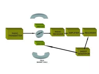
Original Design Data RS232 A/D RF Stages Digital Stages DDS – (Analog Devices) DSP (TI) CPLD (Lattice) Output Filter Data and Address Bus Data and Control Signals Clock 50 or 60 MHz Vector Signal Analyzer RF amp Antenna
DSP - TI • TMS320C54 Evaluation Board (Spectrum Digital) • TMS320549 TI DSP Processor • Controls configuration and handles data flow • Easily reprogramable for different modulation schemes • Room for expansion • Powerful processor • Large amount of memory
DSP Problems • Different version of Spectrum Digital’s evaluation board than ECE320 • Incompatible PC driver software • Available sample / test code didn’t work • Poor support from Spectrum Digital • Incorrect driver, software, and information on web site • DSP IO Ports • A/D sample code from Spectrum Digital didn’t work. • RS-232 echo code didn’t work
Final DSP Code • Initializes DDS • Resets DDS on program start • Configures DDS into proper operation mode • Handles communication I/O ports • Prepares input data for output to DDS • Streams data to frequency, phase, or amplitude registers
CPLD Data RS232 A/D RF Stages Digital Stages DDS – (Analog Devices) DSP (TI) CPLD (Lattice) Output Filter Data and Address Bus Data and Control Signals Clock 50 or 60 MHz Vector Signal Analyzer RF amp Antenna
CPLD • Purpose: • To provide an easy means to reconfigure and rewire the PCB. • Translates Address from the DSP • Contains several state machines that drive control pins on the DDS • Only allows DDS to latch data at the correct time. • “Soft” configuration of DDS
IO Strobe BPSK Reset
CPLD Problems • Broken Test Fixture • Out of Date Web Site • Information was for an older version of the Lattice Semiconductor Programming Software
DDS Data RS232 A/D RF Stages Digital Stages DDS – (Analog Devices) DSP (TI) CPLD (Lattice) Output Filter Data and Address Bus Data and Control Signals Clock 50 or 60 MHz Vector Signal Analyzer RF amp Antenna
DDS • AD 9854 – Direct Digital Synthesizer • Large Amount of Functionality • Quadrature DAC’s • Programmable Clock Multiplier • 48 bit frequency register • 14 bit phase register • 12 bit amplitude register • Ramped FSK and FM CHIRP modes
Block Diagram Data RS232 A/D RF Stages Digital Stages DDS – (Analog Devices) DSP (TI) CPLD (Lattice) Output Filter Data and Address Bus Data and Control Signals Clock 50 or 60 MHz Vector Signal Analyzer RF amp Antenna
RF Stages • Output Filter: - Designed according to frequency band - FM 88-110MHz • RF Amp: - Could be used for more power. • Antenna - Pair of wires
Evolution into a PCB • Proto-board was unreliable • Used schematic to generate a Netlist • Systematically created footprints for the different chips • Individually added all traces according to Netlist • Created Power, Ground and two trace planes
Problems with PCB • Learning to do layout • Missing Clock trace • High mismatch factor at the output due to misplaced resistor
Tests • Carrier Freq Spectrum Output Power = -25dBm @ 104.9 MHz
BPSK Signal BPSK Symbol
FM Radio Modulation • Wanted to actually send a radio signal • We needed a modulation scheme for which there was already a receiver for • FM Audio • DSP has an A/D • FM radio already in the lab
FM Audio 104.9MHz
Future Development • Finish Producing other 3 boards • Give transmitter cards to 320 TA’s • Boost output power via Power Amp. • Build receiver on same board to enable two-way communications • Package and sell • Wireless Modem • Broadcast Radio • Radar • Amateur Radio
Conclusion • Good experience • Fun • Learned about many different things • Dsp’s • RF • Board Layout • Digital Circuitry • Modulation Schemes
Questions? • We know you have them…