
Understanding Operational Amplifiers: Analysis and Applications
This module provides an in-depth review of operational amplifiers (op-amps), focusing on their ideal characteristics and applications. It covers key concepts such as negative and positive input-output relationships, power supply voltages, and the equivalent circuit model. Learn about the significance of infinite input resistance (rin), gain (Av), and the conditions for linear operation. Explore practical examples including non-inverting and inverting amplifiers, summation amplifiers, and difference amplifiers, illustrating the ideal op-amp approximation for simplified circuit analysis.

Understanding Operational Amplifiers: Analysis and Applications
E N D
Presentation Transcript
Review from Operational Amplifiers I: Negative input Output Positive input Power SupplyVoltages Anatomy of an “Op-Amp” VPOS –VNEG
vOUT v+ Av(v+– v–) rin v– These features motivate the Ideal Op-Ampapproximation Equivalent model for the circuit inside an op-amp Dependent Source Model • rin is on the order of several Megohms: • Av is on the order of 105 to 106
Vpos Upper Limit Range Lower Limit –Vneg Dependent Source Model • vOUT must lie between Vpos and –Vneg VPOS vOUT –VNEG • Otherwise, the op-amp becomes saturated. • Saturated op-amp vOUT = Vpos or –Vneg limit
VPOS –VNEG vOUT v+ rin = Av = Very Large v– The Ideal Op-Amp Approximation rin= –Vneg < VOUT < Vpos This model greatly simplifies op-amp analysis
i+ = 0 i= 0 A Consequence of Infinite rin VPOS rin= VNEG Currents i+ and ito (or from) input terminals are zero
Defines the Linear Region of operation A Consequence of Large Av If vOUT lies between Vpos and –Vneg … (v+ v–) 0 VPOS –VNEG
vOUT vOUT = = R1 +R2 R1 +R2 vIN vIN R1 R1 (works because i = 0) R1 R1 Via voltage division v– = vOUT vIN= vOUT R1 +R2 R1 +R2 When vOUT in linear region: –vneg< vOUT < vPos Example: The Non-Inverting Amplifier Revisited vIN vOUT R2 i = 0 R1 Use the Ideal Op-Amp approximation: v vIN Done!
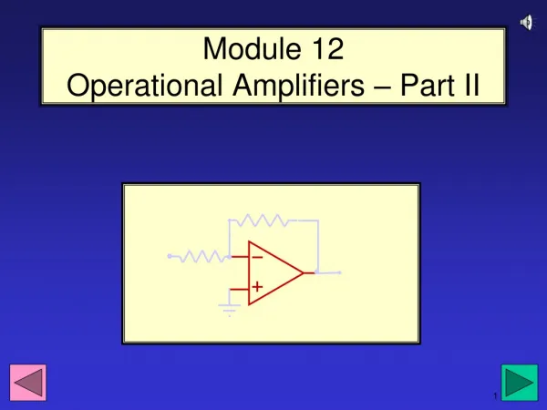
i1 i = 0 vIN = vIN v i1 = R1 R1 Via KCL R2 vOUT = vIN R1 vOUT = vIN R2 R1 Example: The Inverting Amplifier Revisited + – i2 R2 vIN vOUT R1 Use the Ideal Op-Amp approximation: v 0 v+ = 0 Ohm’s Law i1 = i2 (with i = 0) vOUT = i2 R2 = i1 R2 Done!
iF i1 i2 RF R1 R2 + _ v1 + _ v2 + – vOUT i1 + i2 = iF KCL: v1 v1 v2 v2 RF RF vOUT = v1 + v2 i2 = i1 = iF = + R2 R1 R1 R2 R1 R2 vOUT = iFRF Another Example: The Summation Amplifier + – Use the Ideal Op-Amp Approximation… Output is weighted, inverted sum of inputs
iF i2 i1 RF R1 R2 v3 vn v1 R3 + + + + . . . _ _ _ _ v2 + – Rn vOUT vOUT = v1 + v2 + v3 + …+ vn RF RF RF RF R1 R3 Rn R2 Can extend result to arbitrary number of input resistors: Output is weighted, inverted sum of inputs: iF = i1 + i2 + i3+ … + in
R2 R1 + _ + – v1 R1 + vOUT _ v2 R2 Another Example: DifferenceAmplifier
+ – vOUT vOUT = v1 R2 R1 1st Partial result for vOUT Use Superposition: R2 R1 + _ v1 R1 + _ v2 R2 Set v2 to zero i+ = 0 v+ = 0 v = 0 We have an inverting amplifier
i+ + – vOUT R2 v+ = v2 R1 +R2 2nd Partial result for vOUT R2 R1 +R2 R1 +R2 R2 vOUT v+ = v2 = v2 = R1 +R2 R1 R1 R1 Use Superposition, con’t: R2 R1 + _ v1 R1 + _ v2 R2 Set v1 to zero Via voltage division We have an non-inverting amplifier
+ – vOUT R2 vOUT = v2 v1 R1 R2 R2 R1 vOUT = (v2 v1) R1 R2 R1 + _ v1 R1 + _ v2 R2 Add together the 2nd and 1st partial results: Amplifies difference between v2 and v1
vOUT = v1 + v2 + v3 + …+ vn RF RF RF RF R2 R1 R3 Rn R2 vOUT = (v2 v1) R1 Summary • Ideal Op-Amp Approximation simplifies circuit analysis • “Ideal” impliesrin = andv+ = vin the linear region • Summation Amplifier • Difference Amplifier
End of This Module Homework