Download
1 / 16
160 likes | 179 Vues
This technical workshop discusses the use of InfiniBand technology on FPGA to handle high data volumes in the LHCb (large hadron collider) detector. The workshop explores the challenges and benefits of implementing InfiniBand in the trigger and data acquisition systems.

E N D
LHCb and InfiniBand on FPGA Niko Neufeld
Motivation • The LHC (large hadron collider) collides protons every 25 ns (40 MHz) • Each collision produces about 100 kB of data in the (upgraded) detector • Currently a pre-selection in custom electronics rejects 97.5% of these events unfortunately a lot of them contain interesting physics • In 2017 the detector will be changed so that all events can be read-out into a standard compute platform for detailed inspection Technical WS on InfiniBand in Trigger&DAQ - LHCb and IB on FPGA
Key figures • Minimum required bandwidth: > 32 Tbit/s • # of 100 Gigabit/s links > 320 • # of compute units > 1500 • An event (“snapshot of a collision”) is about 100 kB of data • # of events processed every second: 10 to 40 millions • # of events retained after filtering: 20000 to 30000 (data reduction of at least a factor 1000) Technical WS on InfiniBand in Trigger&DAQ - LHCb and IB on FPGA
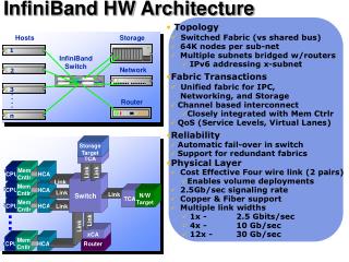
Dataflow Detector • GBT: custom radiation- hard link over MMF, 3.2 Gbit/s (about 12000) • Input into DAQ network (10/40 Gigabit Ethernet or FDR IB) (1000 to 4000) • Output from DAQ network into compute unit clusters (100 Gbit Ethernet / EDR IB) (200 to 400 links) Readout Units 100 m rock DAQ network Compute Units Technical WS on InfiniBand in Trigger&DAQ - LHCb and IB on FPGA
Event-building Detector • GBT: custom radiation- hard link over MMF, 3.2 Gbit/s (about 10000) • Input into DAQ network (10/40 Gigabit Ethernet or FDR IB) (1000 to 4000) • Output from DAQ network into compute unit clusters (100 Gbit Ethernet / EDR IB) (200 to 400 links) Readout Units send to Compute Units Compute Units receive passively “Push-architecture” Readout Units 100 m rock DAQ network Compute Units Technical WS on InfiniBand in Trigger&DAQ - LHCb and IB on FPGA
Deployment • System needs to be ready for detector commissioning in 2018 • Acquisition and deployment of 1/3 of network + 1/6 of compute-nodes in 2017 • Additional compute nodes acquisitioned and installed by end of 2018 • More compute nodes as money comes in and accelerator ramps up Technical WS on InfiniBand in Trigger&DAQ - LHCb and IB on FPGA
Compute Unit • A compute unit is a destination for the event-data fragments from the readout units • It assembles the fragments into a complete “event” and runs various selection algorithms on this event • About 0.1 % of events is retained • A compute unit will be a high-density server platform (mainboard with standard CPUs), probably augmented with a co-processor card (like Intel MIC or GPU) Technical WS on InfiniBand in Trigger&DAQ - LHCb and IB on FPGA
Readout Unit • Readout Unit needs to collect custom-links • Some pre-processing • Buffering • Coalescing of data-fragment reduce message-rate / transport overheads • Needs an FPGA • Sends data using standard network protocol (IB, Ethernet) • Sending of data can be done directly from the FPGA or via a standard network silicon • Works together with Compute Units to build events Technical WS on InfiniBand in Trigger&DAQ - LHCb and IB on FPGA
Challenges • LHCb compute unit needs to handle about 100 Gbit/s (to keep number reasonably low) • Data-transport of 32 Tbit/s over 200 m • Current 100 Gbit/s PHY standards either too short (SR-10) or too expensive (LR-4) • 40 and 10 Gigabit standards require a lot of optical links and switch ports Technical WS on InfiniBand in Trigger&DAQ - LHCb and IB on FPGA
The case for InfiniBand • Cost of switch ports excluding optics • Edge ports are ports with shallow buffers (cut-through) and without high-speed uplinks • Core ports are ports with deep buffers (store and forward) and/or including interconnects and chassis overhead costs Technical WS on InfiniBand in Trigger&DAQ - LHCb and IB on FPGA
Example of IB based read-out • TELL40 using IB FPGA core (Bologna, CERN, …) • 2 FDR IB ports (52 Gb/s) • need16 serializers for about 100 Gbit/s output (can absorb 30 versatile links) • PC using dual-port IB card (Mellanox CX 3) and AMCPCIe converted GBT card • needs PCIe3 16x (1 U PCs with 4 slots exist) Technical WS on InfiniBand in Trigger&DAQ - LHCb and IB on FPGA
InfiniBand: summary • At the bandwidths we need, if it can be shown to work, it will be significantly cheaper ( the core network will be about 33% at today’s best prices) • All arguments for optics / cabling apply in the same way to InfiniBand and Ethernet FDR Infinibandcan transport about 25% more data / fibre and hence needs overall less links additional cost reduction • Definitely important to establish the feasibility of this option (including on FPGA) Technical WS on InfiniBand in Trigger&DAQ - LHCb and IB on FPGA
Basline: Ethernet option Stratix V 24 x GBT • Use 12 x 10 Gigabit Ethernet IP or 3 x 40 Gigabit IP • Effective output bandwidth 120 Gb/s 12 x 10 Gbit/s DDR3 Technical WS on InfiniBand in Trigger&DAQ - LHCb and IB on FPGA
InfiniBand IP Option Stratix V 24 x GBT • InfiniBand Linklayer IP • Made by Polybus Inc. • Currently QDR only • Effective output bandwidth 96 Gbit/s 12 x 10 Gbit/s DDR3 Polybus IP = 3 x QDR Technical WS on InfiniBand in Trigger&DAQ - LHCb and IB on FPGA
ASIC option Stratix V 24 x GBT 12 x 10 Gbit/s DDR3 Stratix V 24 x GBT ConnectX3 16x 8 Gbit/s(PCIe Gen 3) 2 x FDR = 8 x 14 Gbit/s • Larger board needed • Needs more (slower) serializers • Need PCIe bridge or x16 softcore • Effective output bandwidth 104 Gbit/s DDR3 Technical WS on InfiniBand in Trigger&DAQ - LHCb and IB on FPGA
InfiniBand on custom electronics: summary • Can use Mellanox ASIC or • Polybus IP • Both options have advantages and disadvantages from a board-design point of view • In any case need a Subnet Manager Agent (SMA) and a some additional software (available in open-source) most likely easiest to implement using a micro-controller (NIOS) • Cost advantage of IB must offset additional cost and complexity in Readout Unit layer Technical WS on InfiniBand in Trigger&DAQ - LHCb and IB on FPGA