Download

1 / 15
150 likes | 315 Vues
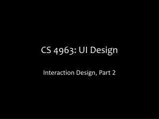
EE 466/586 VLSI Design. Partha Pande School of EECS Washington State University pande@eecs.wsu.edu. Lecture 17 Sequential Logic (Cont’d). CLK. CLK. A. B. D. T. I. T. I. Q. 1. 1. 2. 3. c 1. c 2. CLK. CLK. Dynamic Latches and Registers.

E N D
EE 466/586VLSI Design Partha Pande School of EECS Washington State University pande@eecs.wsu.edu
Lecture 17 Sequential Logic (Cont’d)
CLK CLK A B D T I T I Q 1 1 2 3 c1 c2 CLK CLK Dynamic Latches and Registers • The setup time of this circuit is the delay of the transmission gate. • It is the time taken by node A to sample the D input. • The hold time is approximately zero, as the T1 is turned off on the clock edge and further input changes are ignored. • The propagation delay (tc-q) is equal to two inverter delays plus the delay of T2.
Clock Overlap • During the 0-0 overlap period, the PMOS of T1 and the PMOS of T2 are simultaneously on • A direct path for data to flow from the D input of the register to the Q output • Race condition • The output Q can change on the falling edge if the overlap period is large • Undesirable effect for a positive edge triggered register. • For 1-1 overlap region • Path exists through NMOS of T1and the NMOS of T2.
Clock Overlap (Cont’d) • 1-1 Overlap • Taken care of by enforcing a hold time constraint. • Data must be stable during the high-overlap period. • 0-0 Overlap • Make sure that there is enough delay between the D input and node B • Ensure that the new data sampled by the master stage does not propagate through to the slave stage.
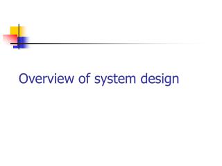
Other Latches/Registers: C2MOS “Keepers” can be added to make circuit pseudo-static
Insensitive to Clock-Overlap V V V V DD DD DD DD M M M M 2 6 2 6 M M 0 0 4 8 X X D Q D Q M M 1 1 3 7 M M M M 1 5 1 5 (a) (0-0) overlap (b) (1-1) overlap
Other Latches/Registers: TSPC Positive latch (transparent when CLK= 1) Negative latch (transparent when CLK= 0)
Including Logic in TSPC Example: logic inside the latch AND latch
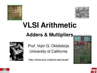
Pulse-Triggered LatchesAn Alternative Approach Ways to design an edge-triggered sequential cell: Master-Slave Latches Pulse-Triggered Latch L1 L2 L Data Data D Q D Q D Q Clk Clk Clk Clk Clk
Pulsed Latches Hybrid Latch – Flip-flop (HLFF), AMD K-6 and K-7 :