Download

1 / 18
180 likes | 866 Vues
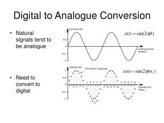
Digital to Analogue Conversion. Analogue Digital Conversion . Analog and digital data were briefly mentioned at the start A digital signal is an approximation of an analog one Levels of signal are sampled and converted to a discrete bit pattern.

E N D
Analogue Digital Conversion • Analog and digital data were briefly mentioned at the start • A digital signal is an approximation of an analog one • Levels of signal are sampled and converted to a discrete bit pattern. • Digital signal processing is used, for example, to enhance and compress images, to process sounds to generate speech, etc, etc.
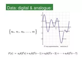
Step (discrete) Approximation “stair-step” approximation of original signal sample level more samples give greater accuracy time hold time for sample
Objectives • To understand how a digital value can be converted to an analogue value • To draw circuits and explain the operation of two digital to analogue converters: the binary weighted resistor network and the R-2R ladder network • To draw the block diagram and explain the operation of three analogue to digital converters: flash, counter ramp and successive approximation • To be able to calculate the conversion time for an analogue to digital converter • To be able to explain the sampling rule • To be able to describe the basic design of a sample and hold circuit and explain how it works
The binary weighted resistor network • Comprises of a register and resistor network • Output of each bit of the register will depend on whether a 1 or a 0 is stored in that position • e.g. for a 0 then 0V output • for a 1 then 5V output • Resistance R is inversely proportional to binary weight of each digit R MSB 4-bit register RL 2R VL 4R 8R LSB
Buffering the resistor network • Best solution is to follow the resistor network with a buffer amplifier • Has high impedance, practically no current flows • All input currents sum at S and go through Rf • Vo = -IfRf V = - I ´ R = - ( I + I + I + I ) ´ R o f f 1 2 3 4 f
Digital-to-Analogue Example • Calculate the output voltage for an input code word 0110 if a logic 1 is 10V and a logic 0 is 0V, and R = RF=1k • I1 = I4 = 0 • I2 = 10v / 2R = 10 / 2k = 5 mA • I3 = 10v / 4R = 10 / 4k = 0.25 mA • Vo = -If x Rf = -(0.0075) x 1000 = -7.5 volts V = - I ´ R = - ( I + I + I + I ) ´ R o f f 1 2 3 4 f
The binary weighted resistor network • Seldom used when more than 6 bits in the code word • to illustrate the problem consider the design of an 8-bit DAC if the smallest resistor has resistance R • what would be the value of the largest resistor? • what would be the tolerance of the smallest resistor? • Very difficult to manufacture very accurate resistors over this range
The R-2R Ladder Resistor Network • Has a resistor network which requires resistance values that differ 2:1 for any sized code word • The principle of the network is based on Kirchhoff's current rule • The current entering N must leave by way of the two resistors R1 and R2 •
The R-2R Ladder Resistor Network • Works on a current dividing network • Resistance to right of B = 1/(1/2R + 1/2R) • Resistance to right of A = R +2R/2 = 2R • Current divides I1 = I/2 I2 = I/4 divides again
The R-2R Ladder Resistor Network • The network of resistors to the right of A have an equivalent resistance of 2R, and so the right hand resistance can be replaced by a copy of the network Bit Current 3 I/2 2 I/4 1 I/8 0 I/16 bit 3 bit 2 bit 1 bit 0
The R-2R Ladder Resistor Network The state of the bits is used to switch a voltage source V = -R ( b I 2 + b I 4 + b I 8 + b I 16 ) 1 o f 3 2 0
Example • For the circuit shown above with I = 10 mA and Rf = 2k, calculate the output voltage V0 for an input code word 1110. V = -R ( b I 2 + b I 4 + b I 8 + b I 16 ) 1 o f 3 2 0
Example • I = 10mA • Rf = 2k • input code word 1110 Vo = -2000( 0.01/2 + 0.01/4 + 0.01/8 + (0 x 0.1)/8 ) = - 2000 * (0.04 + 0.02 + 0.01) / 8 = 17.5 volts
Quantisation • Suppose we want to use a D-A converter to generate the sawtooth waveform (graph shown on the left) • End up with stair-case waveform (graph shown on the right) • The 16 possible values of the D-A converter output are called the quantisation levels • The difference between two adjacent quantisation levels is termed a quantisation interval
Quantisation Error • Difference between the two waveforms is the quantisation error • Maximum quantisation error is equal to half the quantisation interval • One way to reduce the quantisation error (noise) is to increase the number of bits used by the D-A converter quantisation interval 111 110 101 100 011 010 001 000 bands or quanta 1001 1000 0111 0110 0101 0100 0011 0010 0001 0000 samples
Quantisation Noise • The voltage produced by the DA convertor can be regarded as the original signal plus noise: This is the quantisation noise.
Summary • We have looked at techniques for converting a digital codeword into an analogue voltage using a weighted resistor network. In particular: • the binary weighted network (not suitable for large resolution D-A converters) • the R-2R ladder • The addition of an amplifier minimises the loading effects on the weighted network • The conversion from digital to analogue involves a quantisation process that limits the resolution and introduces the quantisation noise. • This quantisation error can be reduced by increasing the number of bits in the converter.