Vertex detector optimisation: status and strategies
290 likes | 499 Vues
Introduction. Performance goals. Constraints due to machine and detector. Conceptual detector design. Sensors. Mechanical structure. Physics performance. Summary. Vertex detector optimisation: status and strategies. An example of what we want to do:

Vertex detector optimisation: status and strategies
E N D
Presentation Transcript
Introduction. Performance goals. Constraints due to machine and detector. Conceptual detector design. Sensors. Mechanical structure. Physics performance. Summary. Vertex detector optimisation: status and strategies
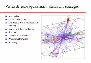
An example of what we want to do: Higgs boson is found, is it evidence for supersymmetry? Measure the branching ratios for decays to b, c and t. Are BRs compatible with the SM... ...or are “d-type” couplings enhanced and “u-type” suppressed as predicted by SUSY? Given expected cross sections and luminosity, measurements require high efficiency b and c identification. Large backgrounds imply high purity needed. If SUSY found, studies often benefit from flavour identification. E.g. scalar top production: followed by Identify b jets plus W decay products (inc. c and b quarks). Introduction
Physics studies can also benefit from separation of E.g. reduce combinatorial background. Also aids study of possible anomalies in gauge boson couplings. Can be observed in angular distributions of W production and decay Favoured process W charge determined from that of m. ID of b and c charges would increase number of channels that could be used in measurement. Charge ID can also make possible measurement of parity of Higgs boson, CP asymmetries in SUSY processes... c W+ e+ e- W- m- Introduction
Average impact parameter of B decay products ~ 300 mm, of charmed particles less than 100 mm. Impact parameter resolution is given by convolution of point precision, multiple scattering effects, lever arm, and mechanical stability. Multiple scattering significant despite large √s at ILC as average charged track momentum 1...2 GeV. Resolve all tracks in dense jets. Cover largest possible solid angle: forward/backward events are of particular significance for studies with polarised beams. Stand-alone reconstruction desirable. In terms of impact parameter, require resolution in rf and rz: Implies typically: Pixels ~ 20 x 20 mm2. First measurement at r ~ 15 mm. Five layers out to radius of about 60 mm, i.e. total ~ 109 pixels Material ~ 0.1% X0 per layer. Detector covers |cos q| < 0.96. Performance goals
Minimum beam pipe radius 14 mm. Pair background at this radius in ~ 4T field causes 0.03 (0.05) hits per BC and mm2 at √s = 500 (800) GeV. Bunch train structure: For pixels of size 20 x 20 mm2, implies readout or storage of signals ~ 20 times during bunch train to obtain occupancy less than ~ 0.3 (0.9) %. Must withstand: Radiation dose due to pair background of ~ 20 krad p.a. Annual dose of neutrons from beam and beamstrahlung dumps ~ 1 x 10⁹ 1 MeV equiv. n/cm2. Must cope with operation in 4T field. Beam-related RF pickup and noise from other detectors may be an issue. 337 (189) ns 0.2 s 2820 (4500) 0.95 ms Constraints due to machine and detector
ILC may be more hostile environment than storage ring. Nanometre beam spots and single pass operation mean invasive diagnostic tools essential, e.g. BPMs, with possible imperfections in shielding of cables, optical ports... Vertex detector is more vulnerable to pickup than other detectors due to: Proximity to beampipe – Faraday cage ideals tend to be compromised. Signals typically only ~ 1000 e-, must be amplified electronically and read out. SLD vertex detector observed massive pickup and optical transmission was disrupted by every bunch: tens of ms needed for recovery. SLD CCD readout strategy: During bunch train, signal charge is stored safely in buried channel. When pickup has died down, charge transferred to output node and sensed as voltage on gate of output transistor. SLD still needed filter which suppressed noise by factor ~ 100. EMI tests later this year at SLAC. Constraints due to machine and detector
Example using CCDs: Surrounded by ~ 2 mm thick Be support cylinder. Allows Be beam pipe to be of thickness of ~ 0.25 mm. Pixel size 20 x 20 mm2, 8 x 108 pixels in total. 50 MHz readout of inner layer. Standalone tracking using outer 4 layers. Hits in first layer improve extrapolation of tracks to IP. Sensor operation at 180 K, gas cooling, additional evaporative cooling for electronics if needed. Readout and drive connections routed along BP. Important that access to vertex detector possible, “roll” outer tracker along BP as done at SLD. Conceptual detector design
Amount of material in active region minimized by locating electronics only at ends of ladders if possible. Resulting material budget, assuming unsupported silicon sensors of thickness ~ 50 mm: Conceptual detector design Material of:beam pipe five CCD layerscryostatsupport shell
Column parallel charge coupled device. First of these, CPCCD1, manufactured by e2v. Two phase, 400 (V) 750 (H) pixels of size 20 20 μm2. Metal strapping of clock gates. Two different gate shapes. Two different implant levels. Wire/bump bond connections to readout chip and external electronics. Direct connections and 2-stage source followers: Direct connections and single stage source followers (20 mm pitch): Sensors – CPCCD (LCFI)
Standalone CPCCD1 tests: Noise ~ 100 e- (60 e- after filter). Minimum clock potential ~1.9 V. Max clock frequency above 25 MHz (design 1 MHz). Limitation caused by asymm. clock signals due to single metal design. Marry with CPCCD readout ASIC, CPR1 (RAL): IBM 0.25 μm process. 250 parallel channels, 20μm pitch. Designed for 50 MHz. Sensors – CPCCD
Wire bonded CPCCD1 – CPR1 assembly. Total noise ~130 electrons. Bump bonding done at VTT: First time e2v CCDs have been bump bonded. Sensors – CPCCD
CPR1 bump bonded to CPCCD1, charge channels: Observe ~ 70 mV signal, expected 80 mV, good agreement. Some teething problems with CPR1. Resolved in CPR2 design which also includes cluster finding logic and sparsified readout. o/p spars. clust. bin. 5-bit ADC pre-amp MPX find conv. Sensors – CPCCD
Next generation, CPCCD2, now being manufactured. Compatible with CPR1 and CPR2. Two charge transport sections. Choice of epitaxial layers for varying depletion depth. Three chip sizes, includes: Large scale stitched devices, area 9.2 x 1.5 cm2, close to ILC size, operate at few MHz. Smaller devices for tests to 50 MHz. No connections this side Stripline clock bus Charge injection Extra pads for clock connection Clock monitoring and extra pads every 5 mm Image area Four 2-stage SF in adjacent columns Standard Field-enhanced Standard Four 1-stage and 2-stage SF in adjacent columns Temperature diode Main clock wire bonds Main clock wire bonds CPR-2 CPR-1 Sensors – CPCCD
High-speed clock propagation, “busline free” CCD. Whole image area serves as distributed bus. Highest speed potential, 50 MHz achievable with suitable driver. Expect robust against pickup as signals “in silicon” until very short paths through bump bonds to CPR. Φ1 Φ2 Φ2 Φ1 To multiple wire bonds Φ1 Φ2 Φ2 Φ1 1 mm To multiple wire bonds Level 1 metal Polyimide Level 2 metal Sensors – CPCCD
Depleted field effect transistor. High resistivity silicon substrate, sensitive over full volume. Electrons collected on internal gate, modulate transistor current. First amplification “in pixel”. 14V Sensors – DEPFET (Bonn, Mannheim, HLL Munich)
Low noise operation possible at room temperature. Double metal structures produced in August 2004, make possible large area sensors. Pixel size 20 x 25 mm2, resolution 9.5 mm. Sensors can be thinned: Sensors – DEPFET Sensor ~ 50 mm Frame ~ 300 mm
Fast steering chip developed (Switcher II) 2 x 64 channels. Sequencer and RAM tested to up to 80 MHz. “Analogue” section (reset signal): Power consumption 1 mW per channel at 30 MHz. 4.8 mm 4.6 mm Sensors – DEPFET
Current Readout (CURO II) chip, 128 channels. Features automatic pedestal subtraction (fast CDS). “On chip“ hit detection and zero suppression. Analogue hit readout works to 50 MHz. Digital processing runs at 110 MHz. Power 2.8 mW per channel. Next steps. Detailed measurements with prototype system: Noise performance. Spatial resolution. Test beam beginning 2005. Improve steering chip, Switcher III: Less static power consumption (power down feature). Analogue operation up to 50MHz. New readout, CURO III, with power down feature. Larger DEPFET matrix (512 x 512 pixels with double metal). Sensors –DEPFET
Monolithic active pixel sensors. Charge collection by diffusion, no field in epitaxial layer. Strasbourg group has developed MIMOSA 1...9, UK group also investigating several designs. MIMOSA 9: 20 m thick epitaxial layer. Cells with 20, 30, 40 m pitch. “Edge” electronics Sensors – MAPS (Strasbourg, DESY and UK groups)
Tested at CERN SPS 120 GeV pions: S/N peak ~ 24 (40 x 40 mm2 pixels). Excellent spatial resolution achieved: Efficiency > 99.8% with 20 x 20 and 30 x 30 mm2 pixels. Sensors – MAPS
Demonstrated that detectors thinned to 15 mm function (MIMOSA 5): Tests suggest MAPS will withstand 0.5...1.0 Mrad, work ongoing. Simulation and measurements of power consumption and cooling underway, e.g. for inner and outer ladders: Thinned Standard Sensors – MAPS
Charge collection time simulated by UK groups. Standard APS2, charge collected from ~ 6 mm layer in about 30 ns. Long compared to readout speeds needed for inner layer of vertex detector, particularly if use thicker epitaxial layer? Solution, deep n well: Allows charge collection in few nanoseconds. Possible decrease in S/N. APS2 in DESY test beam beginning February. APS4 (with deep n well) available from about April. Sensors – MAPS
Fine pixel CCD. Get acceptable occupancy by increasing number of pixels by factor ~ 20 w.r.t. “standard” vertex detector. Pixel size ~ 5 x 5 mm2. Must keep diffusion to minimum so no cluster confusion – deplete full epitaxial layer. Tilt sensors to compensate for spread due to Lorentz angle: Signals “in silicon” during bunch train, readout between bunch trains. Use two CCD sandwich with foam filling to build vertex detector. Hit “doublets” may help in separation of signal from background. Sensors – FPCCD
Flexible active pixel sensors. Add in pixel storage capacitors to MAPS. Present design “proof of principle”. Pixels 20 x 20 mm2, 3 metal layers, 10 storage cells. Pixel not completely full, reducing feature sizes and/or moving to larger pixels will allow more storage cells. Sensors – FAPS (UK groups)
In-situ storage image sensor. Signal always in buried in silicon until bunch train passed. Test device being built by e2v. “Revolver” variant of ISIS reduces number of charge transfers needed, increases radiation hardness and also flexibility of readout. 20 μm 20 μm Sensors – ISIS (LCFI)
Sensors – ISIS 4 5 Storage gate 3 6 Storage gate 2 RSEL OD RD RG 1 7 8 OS Output node to column load Output gate Transfer gate 8 Photogate 20 19 Charge generation Storage Transfer 18 17 Readback from gate 6
Thin ladder design. Unsupported CCD option foundered due to stresses introduced when silicon is processed. Supporting CCD on Be......complicated by requirement that operate at low temperature: Now investigating substrates with thermal expansion close to that of silicon, e.g. carbon fibre and various foams. Studies of ladder end support structures ongoing. Adhesive 0.2mm Beryllium substrate (250 μm) Mechanical considerations (LCFI)
Optimising the physics performance of the vertex detector. Here look again at CCD based system. Study impact parameter resolution in rf, s(d0). Increasing material budget has moderate effect. Performance suffers strongly when beam pipe radius increased from 15 to 25 mm. Physics performance (LCFI)
Many possible sensor technologies are being investigated. Goal of all groups it to demonstrate that these can be operated at the ILC, i.e. that they can achieve the necessary readout speed, that they are insensitive to RF pickup, etc. Tests of full scale ladders required to demonstrate this – progress being made towards this goal. Vertex detectors must be designed around these ladders, providing all necessary services, precision mechanical support, etc. with minimum possible material budget. The physics performance of these “real” detectors must then be evaluated. Simulations should aim to include all possible relevant effects, e.g. fluctuations in deposited charge in thin silicon layers, Lorentz angle, background hits, nuclear counter effect, effects of temperature fluctuations due to power cycling... It should be kept in mind that overall detector considerations (as well as increasing size of silicon wafers!) may lead to changes in the vertex detector design, e.g. an increase in length and/or the addition of a further layer. Summary
