Download
1 / 10
100 likes | 227 Vues
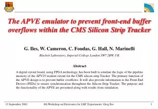
The APVE emulator to prevent front-end buffer overflows within the CMS Silicon Strip Tracker G. Iles, W. Cameron, C. Foudas, G. Hall, N. Marinelli Blackett Laboratory, Imperial College London SW7 2BW, UK. Abstract

E N D
The APVE emulator to prevent front-end buffer overflows within the CMS Silicon Strip Tracker G. Iles, W. Cameron, C. Foudas, G. Hall, N. Marinelli Blackett Laboratory, Imperial College London SW7 2BW, UK Abstract A digital circuit board, using FPGA technology, has been built to emulate the logic of the pipeline memory of the APV25 readout circuit for the CMS silicon strip Tracker. The primary function of the APVE design is to prevent buffer overflows. It will also provide information to the Front End Drivers (FEDs) to ensure synchronisation throughout the Silicon Strip Tracker. The purpose and the functionality of the APVE are presented along with results from simulation. 8th Workshop on Electronics for LHC Experiments: Greg Iles
(1) The CMS Silicon Strip Tracker APV25 readout chip is designed to record analogue data at a rate of 40MHz within the CMS detector. Data are stored in analogue pipelines on the readout chip. Upon reception of a Level 1 Accept (L1A) signal from the Trigger Control System (TCS), they transfer the data via optical links to Front End Driver (FED) cards located in the CMS electronics room. The FEDs digitise the analogue data and employ fast FPGA technology to apply pedestal and noise corrections and reduce the raw data sample by cluster finding. The clustered data are then transmitted to the DAQ via S-links. The CMS Silicon Tracker FED board (9U VME) with transition card for DAQ S-link APV25 silicon strip readout chip silicon strip detector 8th Workshop on Electronics for LHC Experiments: Greg Iles
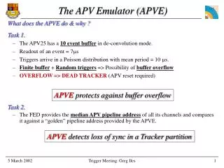
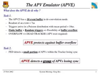
Task 1. The APV25 contains a 192 cell analogue pipeline of which approximately 128 cells are used to buffer data until receipt of a L1A. Up to 31 (peak mode) or 10 (deconvolution mode) of the remaining cells are used to buffer the L1A input rate against the APV25 output rate. The L1A input rate is Poisson distributed with mean period 10us. The APV25 output rate has a constant period of 7us. Random L1As + Finite Buffer + Fixed Output Rate => Buffer Overflow APV25 Buffer Overflow => APV25 Reset Task 2. The FED provides the median APV pipeline cell address of all its 192 channel inputs and compares it against a “golden” pipeline address provided by the APVE. What does APVE do & why ? APVEprotects against buffer overflow APVEdetects loss of sync in a Tracker partition 8th Workshop on Electronics for LHC Experiments: Greg Iles
Preventing buffer overflows in APVs • The TCS sends L1As to the APV. When APV buffers are becoming full the Tracker can assert the status signal BUSY to the TCS. The TCS will then inhibit further L1As. • However, the TCS is allowed to transmit L1As up to every 3 bunch crossings as long as the average rate doesn’t exceed 100kHz. Hence if the control loop ( ) is larger than 3 bunch crossings further L1As may be transmitted before the L1A inhibit acts. There must be APV buffer space for these additional L1As. • Consequently, the larger the control loop the earlier BUSY must be asserted and thus fewer buffers are available to moderate the L1A rate. The consequence is that BUSY is asserted more often and thus the Tracker deadtime increases. The APV buffer query logic must therefore be close to the TCS. L1A Inhibit gate (inside TCS) L1A BUSY APVE: APV buffers full ? The APVE emulates the buffer logic in the APV. It asserts BUSY at a level set by a VME write. It is situated close to the TCS to maintain maximum Tracker efficiency 8th Workshop on Electronics for LHC Experiments: Greg Iles
Control structure • Control & Feedback Structure....... • The APVE receives the LHC clock, control and timing signals ( ) from both a Central & Local TCS. The Local TCS allows the Tracker to operate when the main Trigger system is down for maintenance. A VME write to the APVE determines which, if any, TCS source is selected. • The APVE sends the Tracker status ( ) which may be Busy, Warn, Out-Of-Sync, Ready or Error to the active TCS. The Tracker status is a combination of both the APV and FED status. • The “golden” pipeline address is transmitted to the FED via the TTCci B channel ( ). • APVs in the Tracker receive L1As and control information via the FEC and CCU ring control system. They send data frames ( ), including the pipeline address of each event, to the FEDs CTCS LTCS APVE TTCci/ex/tx FEC FMM CCU Ring Other FEDs APV FED 8th Workshop on Electronics for LHC Experiments: Greg Iles
How does APVE work ? • The APVE monitors APV25 buffer levels via two methods: • Option (i) APV Real • An APV25 on the APVE is fed the same L1A and L1Reset signals as those in the Tracker • A counter keeps track of the number of filled APV25 buffers. • L1A => INCREMENTS • Data frame => DECREMENTS • Reset => CLEARS • The data frame header provides the pipeline address. • Option (ii) APV Sim • An FPGA is used to replicate the internal APV logic. This provides the best Tracker efficiency, but the logic is difficult to synthesise and must match the real APV25 logic precisely. L1A Reset APV Real Real APV25 APV data frame INCREMENT Header recognition CLEAR Frame output signal Buffer counter DECREMENT Assert busy? Busy Pipeline address 8th Workshop on Electronics for LHC Experiments: Greg Iles
Experiment deadtime due to Tracker • The graph shows percentage Tracker deadtime as a function of control loop size (i.e. the time for a L1A from the TCS to reach the APVE and for the BUSY signal to be transmitted back. • Note that below a control loop size of 3 bunch crossings the APV may use all its buffers (10) before asserting BUSY, thus keeping deadtime to a minimum 8th Workshop on Electronics for LHC Experiments: Greg Iles
Pipeline address transmission (I) • APVE “golden” pipeline address transmitted to FEDs by TTC system • The Trigger, Timing and Control (TTC) system distributes to the experiment via a single optical fibre a Clock, and 2 data channels. Channel A is used for L1A transmission whereas channel B is used for control commands. • The “golden” pipeline address will be sent asynchronously via the B channel. It must reach the FED before the FED is ready to check the pipeline address • Pipeline address must not be blocked by synchronous B channel commands for long time period • Solution => Create guaranteed asynchronous bandwidth on B channel of ≥42clks (pipeline address transmission length) every 280clks (APV data frame length). This requires the TCS, that initiates the B commands, and TTCci, that implements the B commands, to follow a few rules. • Rules to guarantee asynchronous bandwidth on channel B • TCS (Central & Local) must separate synchronous B channel commands by ≥88 clk cycles so that a pipeline address may be transmitted between them. • Tracker TTCci must maintain this command separation. All B channel commands must • be initiated by TCS • have the same inhibit duration of 42 clock cycles • TTCci “doubles” are not allowed 8th Workshop on Electronics for LHC Experiments: Greg Iles
Pipeline address transmission (II) TCS initiates command “X” with BGo_X signal. TTCci inhibits new commands from starting for 42clk cycles thus guaranteeing the B channel to be free when the synchronous command “X” is sent. Sync Command “X” is transmitted. BGo_X (1) BGo_Y (1) Inhibit_X (42) Inhibit_X (42) Sync_Y Sync_X (16/42) Pipe Address_B (42) B Chan Data 88clks New B channel command “Y” initiated by TCS after 88clks, but pipeline address “B” is started before inhibit “Y” starts (shaded area) and once started is allowed to complete. 8th Workshop on Electronics for LHC Experiments: Greg Iles
Conclusions • A VME board has been built to prevent buffer overflows in the CMS Tracker. The design of the board and its integration into the CMS control structure ensure that the Tracker deadtime is kept to a minimum. • The deadtime is determined by the magnitude of the control loop formed between the APVE and the TCS and the type of buffer monitoring chosen. The latter can be achieved with either a real APV25 chip or a hardware emulation of the chip in an FPGA. If we assume a TCS-APVE control loop of less than 9 clock cycles these yield a deadtime of less than 0.25% and less than 0.13% respectively. • The APVE will also send information to the FEDs via the TTC B channel to verify that tracker synchronisation has been maintained. APV25 silicon strip readout chip Virtex-II FPGA Interface to TTCci for pipeline address transmission Interface to Central & Local TCS to receive control signals and send status. Additional input for FED status 8th Workshop on Electronics for LHC Experiments: Greg Iles