Development of Scanning Probe Lithography (SPL)
280 likes | 921 Vues
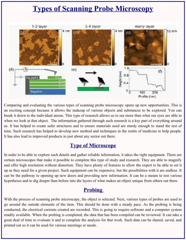
Development of Scanning Probe Lithography (SPL). 1) “ Device fabrication by scanned probe oxidation ”, Science, 1995 2) “ Nanofabrication by scanning probe microscope lithography: A review ”, J. Vac. Sci. Tech., 2005 3) “ Scanning Probe Parallel Nanolithography with Multiprobe Cantilever

Development of Scanning Probe Lithography (SPL)
E N D
Presentation Transcript
Development of Scanning Probe Lithography (SPL) 1) “Device fabrication by scanned probe oxidation”, Science, 1995 2) “Nanofabrication by scanning probe microscope lithography: A review”, J. Vac. Sci. Tech., 2005 3) “Scanning Probe Parallel Nanolithography with Multiprobe Cantilever Array Fabricated by Bulk Silicon Micromachining”, IEEJ, 2008 EE C235/NSE C203 Nanofbrication Jun SukRho
Scanning Probe Lithography • Bottom Up Technique • - Chemical and molecular patterning (DPN) • Top down Technique • - Mechanical Patterning • Scratching • Nano Indentation • - Voltage bias application • Field Enhanced Oxidation • Electron exposure of resist materials • Substitution Technique • - Manipulation of nanostructures Mar. 9th. 2009 Rho, Jun Suk
Achievements Dec. 10th. 2008 Mar. 9th. 2009 Rho, Jun Suk
Scanning Probe Lithography (SPL) Atomic Force Microscopy (AFM) Scanning Tunneling Microscopy (STM) Scanning Probe Parallel Lithography (SPL Array) Dec. 10th. 2008 Mar. 9th. 2009 Rho, Jun Suk
Began at NIST in 1989 Typical line width: below 50nm Scan rate: 10~20um/s Creating patterns with high resolution but are limited in throughput Scanning Probe Lithography (SPL) J. A. Dagata, Vol. 270, pp1625-1626, Science, 1995 Mar. 9th. 2009 Rho, Jun Suk
AFM Lithography Scratching The advantages of nanoscratching for lithography - The absence of additional processing steps (i.e etching) Dec. 10th. 2008 Mar. 9th. 2009 Rho, Jun Suk
Electric Field Enhanced Oxidation • Voltage bias between a sharp probe tip and sample • generates an intense electric field at the tip • Oxidization of silicon & Anodization of metals • The high field desorbs the hydrogen on the silicon • surface and enables exposed silicon to oxidize • Oxidation depends on humidity • Can achieve sub-50nm feature sizes J. A. Dagata, Vol. 270, pp1625-1626, Science, 1995 Dec. 10th. 2008 Mar. 9th. 2009 Rho, Jun Suk
Scanned Probe Oxidation- Applications Fabrication of single tunneling transistor(SET) Fabrication of Si nanowire J. A. Dagata, Vol. 270, pp1625-1626, Science, 1995 Mar. 9th. 2009 Rho, Jun Suk
Electric Field Enhanced Oxidation AFM anodic Oxidation (Left) AFM Nanolithography (Below) Dec. 10th. 2008 Mar. 9th. 2009 Rho, Jun Suk
Parallel Field Enhanced Oxidation Dec. 10th. 2008 Mar. 9th. 2009 Rho, Jun Suk
Profile vs. Resist by AFM Lithography M. Rolandi et al. NANOLETTERS. 2004Vol. 4, No. 5889-893 Mar. 9th. 2009 Rho, Jun Suk
Non Contact AFM Lithography • Silicon probe tip acts as a source of electrons • The field emission current from the tip is used as the • feedback signal to control the tip sample spacing Dec. 10th. 2008 Mar. 9th. 2009 Rho, Jun Suk
Pros & Cons of SPL (AFM Lithography) Pros • Making nano patterns without optical apparatus • Making arbitrary patterns by controlling AFM tips • Good linearity allowing excellent line width control • No backscattering which exists in EBL • No proximity which exists in EBL Cons • Low throughput: serial scan and low speed • Small scan area • Requires higher incident electron dose than EBL Mar. 9th. 2009 Rho, Jun Suk
Scanning Probe Lithography (SPL) Atomic Force Microscopy (AFM) Scanning Tunneling Microscopy (STM) Scanning Probe Parallel Lithography (SPL Array) Dec. 10th. 2008 Mar. 9th. 2009 Rho, Jun Suk
1D tunneling Dec. 10th. 2008 Mar. 9th. 2009 Rho, Jun Suk
STM Lithography • Application of voltage pulse between tip and sample • “Pushing” atoms • Advantages of STM Litho • Information storage devices • Nanometer patterning atoms M. Crommie (UC Berkley), Vol. 262, Science, 1993 Dec. 10th. 2008 Mar. 9th. 2009 Rho, Jun Suk
Scanning Probe Lithography (SPL) Atomic Force Microscopy (AFM) Scanning Tunneling Microscopy (STM) Scanning Probe Parallel Lithography (SPL Array) Dec. 10th. 2008 Mar. 9th. 2009 Rho, Jun Suk
Scanning Probe Arrays Lithography HensyGandjar, Yuki Takagi, Naoki Matsuzuka, YoshitadaIsono, IEEJ, 2008 Mar. 9th. 2009 Rho, Jun Suk
Scanning Probe Arrays Lithography HensyGandjar, Yuki Takagi, Naoki Matsuzuka, YoshitadaIsono, IEEJ, 2008 Mar. 9th. 2009 Rho, Jun Suk
Comparison Mar. 9th. 2009 Rho, Jun Suk
Conclusion Although Several basic issues are still unresolved with respect to these techniques, (i.e. the details of The mechanism of ink transport in DPN are still unclear), it is very promising and developing technique. Polymer Pen Lithography SPL with NSOM SPL with SECM Self Assembly Monolayer (SAM) ETC On-wire Lithography Dec. 10th. 2008 Mar. 9th. 2009 Rho, Jun Suk
Thank You ! Dec. 10th. 2008 Mar. 9th. 2009 Rho, Jun Suk